I am repairing a "James" subwoofer model 6 amplifier "see schematc". I got it running, but it has 13% distortion and the output filters are hot, 100 degree C.
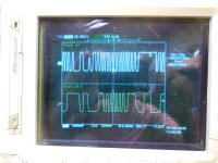
It is a bridged design and the (pos side) pwm is 1.8 khz IC13 pin 6 while the (neg side) pwm IC 4 pin 6 is 360hz. Shouldn't these signals be the same?
Thanks, Gary
It is a bridged design and the (pos side) pwm is 1.8 khz IC13 pin 6 while the (neg side) pwm IC 4 pin 6 is 360hz. Shouldn't these signals be the same?
Thanks, Gary
Attachments
Yes. Both channels should have a similar switching frequency. The inductors are hot because the ripple current must be very high. Maybe one of the output FETs is open or shorted or not switching causing a very low or a very high duty cycle and a low frequency in the self ocscillating circuit.
Thanks, All the FET's have been replaced, but I blew one of the output FETs when I dis-connected R143 to test IC13 which was bad. I could still have a bad FET. I'll look at it and follow-up.

IC13 could go bad but it is more likely that some component in the switching output circuit went bad because that is where the components get stressed with temperature, voltage and current. If the output blew up after removing the feedback resistor R143 then IC13 was likely working and still controlling the switching loop in some failed condition. The presence of R143 should not matter if IC13 was bad and not controlling the loop.
I think that you went too far. You are testing parts from both channels when only one channel was probably bad. There is no reason to check the parts in the good channel. You should be looking at the channel with the low frequency. You could use the good channel as a reference to see what is different in the other channel. You can compare in circuit resistor measurements of the 2 channels and look for differences. Check the resistance of every node to ground and compare them. Check every resistor for opens and every capacitor for shorts, Test each diode. Much of the testing can be done with the parts still on the board. When a difference between channels is found then you should look closer. If the FETs are good then you are left with testing the smaller drive components.
I did take measurements of all the resistors diodes and capacitors on the board with the transistors removed and did not find any differences or out of value parts. I will re-assemble with the other op-amp (IC4) replaced and will focus on the low frequency output as you suggested.
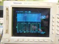
It seems to me that the issue is with IC 10,11 & 12. Can I run this amp with the output filters disconnected at "out 1" & "out Y" without it blowing up?
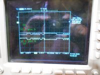
Have you checked to see if you have +5v and -5v on IC4 and if SD5V is 5v? Check the voltage on pin 8 of IC11 and IC12 and pin 1 of IC10. Also, you show a 16V power supply on your outputs. Is this right? I don't understand your plots with a light blue and a dark blue trace. Why are there two traces on one output? The outputs look like they are similar at this point. The frequency is about 2.5 khz for both channels and that is too low. I suspect a power supply problem at this point because both channels look similar. Yes. You could disconnect the output filters without harming the outputs but I doubt that it is necessary. Just power it up for short periods of time to take your data.. If it hasn't blown up during your testing then it is not too stressed.
Last edited:
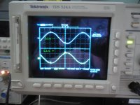
Just re-checked +/-5v okay. SD5V is 63v BINGO. I will find out why. The two traces "sine waves" are the line input to each side of the bridge (positive) amp and (negative amp) signifying the preamp is supplying the proper inverted inputs. the attached traces are the IR2011s output driver and are messed up probably because of the bad SD5v.
Attachments

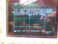
I'm not sure what to look at next. IC1 and IC10 top and bottom traces Pin 3 vs Pin 8 should be the same gain and they are not. They are inverted though. At this point, I agree it could be a power supply problem, The power supply design is very difficult for me to understand and troubleshoot.
Measure the voltage between pin 8 and pin 4 on IC12. It should be 5V or no more than 7V. Did you verify the rail to rail output voltage of 16v on your output? It think it should be about 120V. I am pretty sure that there is a problem with the power for IC11 and IC12.
Last edited:
There is a P_C signal that comes from R_CUT that may be doing something. It seems that this signal affects the output logic of both channels through D7 and D19 until the 15V+ supply is up. That may be the common point that is shutting down the lower power FETs of both channels. Maybe the PC17K opto-coupler is leaky or shorted.
- Home
- Amplifiers
- Class D
- Help! Fixing a "James" Discrete Class D BTL Subwoofer Amplifier