well , make up your mind ....... you're not having voltage at 240 ........ or on 9240 ?

change them both ,they're anyway peanuts price , vs. everything else
change them both ,they're anyway peanuts price , vs. everything else


we can give you guides and tips
footwork is all yours ........ considering that we aren't exactly in neighborhood
sorry , I can't check your pcbs , even if given so nicely ....... it seems I have some sort of mental blockade ...... able to do that only in vivo , on gadget I'm actually repairing
footwork is all yours ........ considering that we aren't exactly in neighborhood
sorry , I can't check your pcbs , even if given so nicely ....... it seems I have some sort of mental blockade ...... able to do that only in vivo , on gadget I'm actually repairing
I glean the following from the posts above:
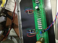
1. You mirrored the layout between the two boards, and
2. You found that the ZTX550 was incorrectly installed (quite possibly due to the mirroring).
Have you checked that the MOSFETs are correctly installed? Notice on your mirrored (bottom) layout that the MOSFETs have their gate pin on the right, while the top layout has the gate pin on the left. You'll need to install MOSFETs rotated 180-degrees oln the mirrored board in order to get anything out of them. This, unfortunately, puts their mounting screw under the PCB, so you'll have to heatsink them before you solder them on.
I agree. You might want to cut the traces on right channel's PCB leading to Mosfets and use short wires for those connections.
no need for cutting anything
just rising pcb little more ,mosfet legs not bent , then short wires leading from legs to proper pads
just rising pcb little more ,mosfet legs not bent , then short wires leading from legs to proper pads

needtubes,you are the savior!!!!
3D fooled me and the designer.Thanks a bunch for all of you.I will redesign the PCB. I think the guy who made it has to work on it.
.......
are you absolutely sure that right pcb is flawless in design ?.........


Nice! Are you going to correct the right channel boards you previously shipped?And this worked. Thank you all. More attention to detail next time.And it is wonderful as expected. Papa's most unique and wonderful creations.
yup Vlad,I will have to get it made again. Option either whole new set for half price or just left channel for free. Please send me a PM.
Last edited:
I would opt for a new set at half price.yup Vlad,I will have to get it made again. Option either whole new set for half price or just left for free.
- Status
- Not open for further replies.
- Home
- Amplifiers
- Pass Labs
- Help! F2 /F2J Issue