Help! F2 /F2J Issue-Resolved
Hi guys,
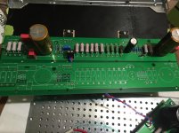
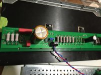
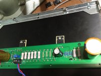
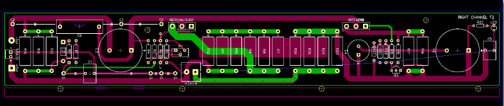
Finally I got to make my F2's right channel. Unfortuantely am not able to make it work.I did complete left channel and working fine. PCB are made by myself but should not be the reason as the left if working fine
How should I start trouble shooting?
I started with F2J on right side as I did F2 on left. Now when it is not working I changed my SJEP JFEt and put 100K for R6 and put R2 and Zener back.
There is 25Volt supply and reading 8v across C-E pins of ZTX550. But cant get any other voltages. What should I be looking for?Spent almost 3 hours changing of mosfets etc. No luck.
Any suggestions?
Found out to be layout issue. Made it work but will get new ones made.
Hi guys,
Finally I got to make my F2's right channel. Unfortuantely am not able to make it work.I did complete left channel and working fine. PCB are made by myself but should not be the reason as the left if working fine
How should I start trouble shooting?
I started with F2J on right side as I did F2 on left. Now when it is not working I changed my SJEP JFEt and put 100K for R6 and put R2 and Zener back.
There is 25Volt supply and reading 8v across C-E pins of ZTX550. But cant get any other voltages. What should I be looking for?Spent almost 3 hours changing of mosfets etc. No luck.
Any suggestions?
Found out to be layout issue. Made it work but will get new ones made.
Last edited:
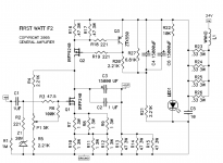
It is the standard schematic of F2. Not sure where I messed up. But happy to hear from you Zen mod!
Placed an empty PCB to make comparison easier.
Placed an empty PCB to make comparison easier.
Attachments

Last edited:
OK , you made pcbs
are you absolutely sure that right pcb is flawless in design ?
also - that design is sorta familiar ....... I believe there was a thread someone doing amp with these pcbs ?
are you absolutely sure that right pcb is flawless in design ?
also - that design is sorta familiar ....... I believe there was a thread someone doing amp with these pcbs ?
I believe so, they should be as the left Chanel is working fine. It was probably me as no one else was making these PCBs recently.
I just double checked everything on board. It is an exact copy of left channel.
What happens if pins of ztx550 get reversed? I am having hard time with this package. But again it is working fine the way it is on left channel.
What happens if pins of ztx550 get reversed? I am having hard time with this package. But again it is working fine the way it is on left channel.
I do t think it is reversed, I checked with multimeter to confirms ( BE junction has higher voltage reading ). The ZTX550 has a flat face and semi flat face where they put the marking on. Usually flat surface faces us when reading the pin out configuration. But that surface also will have device labeling. Here the flatter surface is empty with a dot.
if you really have a problem with pinout of part , buy one of cheap universal testers
those shiny "LRCand everything" .... , like this one : 2017 Version Transistor Tester LCR Diode Capacitance ESR meter Signal Generator | eBay
ZTX550 - semi flat face to you , legs down
from left to right C , B , E (according to ECA VRT Database)
those shiny "LRCand everything" .... , like this one : 2017 Version Transistor Tester LCR Diode Capacitance ESR meter Signal Generator | eBay
ZTX550 - semi flat face to you , legs down
from left to right C , B , E (according to ECA VRT Database)
go to first watt site , look for articles , download and read mosfet matching
remove mosfets from pcb , test them
or simply put new ones , same as new ZTX550
if pcb is OK , and if you didn't burned (really hard to do with that schmtc) some resistor, it should work
remove mosfets from pcb , test them
or simply put new ones , same as new ZTX550
if pcb is OK , and if you didn't burned (really hard to do with that schmtc) some resistor, it should work
After changing ZTX 550 I am getting ~18V between C-E pins, the working board only shows 5.5V between C-E of ZTX 550.
Hi Kinku I would seriously recheck and resolder some of your joints. Looking at the first output device there is not enough solder to make good contact.

Thanks Formantjim.
There is no voltage between irfp9240 gate and source for the faulty board. There 4.9V between Source and gate for both IRF240 and IRF9240 in working board?😕.
There is no voltage between irfp9240 gate and source for the faulty board. There 4.9V between Source and gate for both IRF240 and IRF9240 in working board?😕.
check R20, R21, R27 and traces for them
not fastest but somehow easiest approach - comparing good and bad channel - take ohm reading across every resistor
of course , amp off 🙂
write here when you find something suspicious
not fastest but somehow easiest approach - comparing good and bad channel - take ohm reading across every resistor
of course , amp off 🙂
write here when you find something suspicious
Last edited:
check R20, R21, R27 and traces for them
not fastest but somehow easiest approach - comparing good and bad channel - take ohm reading across every resistor
of course , amp off 🙂
write here when you find something suspicious
I checked twice for resistors, except R21 I guess charging cap shows climbing resistance in both channels. Nothing suspecious in values .
Voltage now exists between source and gate of IRFP9240, about 18V
Wish I know what is wrong?
Last edited:
- Status
- Not open for further replies.
- Home
- Amplifiers
- Pass Labs
- Help! F2 /F2J Issue