Ok, but you might spot check other reading to confirm nothing has changed, especially Q32 collector.
Q32 base and collector: 0.7/1.6
Q10 base, emitter, collector: 1.2/1.1/0.9
Q8 base: 0.3/0.7/0.9
Junction of R65 and R53 (set pot for maximum resistance): 1.2
Top of R66: 1.4
Bottom R49: 0.3
Any thoughts?
Again, I really appreciate all the time, effort and knowledge that you are contributing for me as a result of a dumb mistake. Thanks so much🙏.
Well, there are several very strange readings.
The bases of Q10 and Q8 have 0.9V separating them; the voltage between them should be divided by R65 and R53, but the 1.2V (same voltage as Q10 base) at their junction suggests there's no current through R53. An open pot, or a broken trace at either end of the pot? I suggest resolving that mystery first. Don't I recall a fried pot mentioned in an earlier post? Once corrected, you might retest the spreader to see if it behaves.
Assuming oddities persist after the resistor chain is repaired, both Q8 and Q10 present some odd voltages. It might be easiest to test both transistors out of circuit. And with both transistors out-of-circuit, resistance tracing will be easer, too. Trace the resistor and diode path from Q10 collector through Q14 sense diode, R66, R65, R53, R49, Q3 sense diode back to Q32 emitter. There should be continuity along the entire path. Then with Q8, Q10 back in place, recheck spreader voltages.
All terminal voltages at Q10 are odd--- there's not enough base-emitter voltage on Q10 to cause collector current to flow. The most glaring discrepancy is below (post 82): the first line indicates Q32 collector voltage is 1.6V, and the second line says Q10 collector is 0.9V. But the schematic indicates they are supposed to be the same circuit node. Perhaps there's a broken trace between the two points?
Even if Q10's collector lead is open, it's hard to see a viable bias path to Q8 and thus into Q32 base. I suggest inspecting continuity path between Q10 and Q32 collectors. Also test Q10 out of circuit for possible failure.
Q32 base and collector: 0.7/1.6
Q10 base, emitter, collector: 1.2/1.1/0.9
Even if Q10's collector lead is open, it's hard to see a viable bias path to Q8 and thus into Q32 base. I suggest inspecting continuity path between Q10 and Q32 collectors. Also test Q10 out of circuit for possible failure.
With the R53 pot adjusted for maximum 200 ohm, I estimate the spreader voltage across Q32 should be about 3.318V; if R53 resistance is reduced, spreader voltage will increase.
I'll try to explain the operation of this spreader with the hope that understanding its principles will aid troubleshooting.
Of course, the purpose of the spreader is to generate the base voltages that drive the output stages; in the case of this amplifier, the output design uses three cascaded emitter followers and their complimentary brethren. In rough numbers, each of the 6 devices needs about 0.6V base-emitter to begin conduction--- roughly 3.6V The transistors in the spreader are thermally coupled to the output transistors so that the spreader voltage "tracks" temperature changes in the power devices. The scheme manages bias current to minimize crossover distortion. It's a vast topic, but I hope this is enough summary for present description.
In this bias spreader, thermal-track diodes in the Q14 and Q3 transistors are temperature sensors along with the Vbe junctions in Q10 and Q8. Collector current flowing in Q10 and Q8 controls base current into Q32. These three transistors form a temperature-sensitive shunt regulator that sets the spreader voltage. Resistors R66, R65, R53, and R49 control the gain that multiplies the junction voltages--- thus the "Vbe multiplier" label that's often given.
So here's how the voltage was estimated. Transistors are assumed ideal--- lots of gain, no base current, and 0.6Vbe.
At equilibrium, there must be 1.2V between the bases of Q10 and Q8.
The current through R65+R53 is thus 1.2V/(R65+R53) = 2.55mA.
Voltage across R49 = voltage across R66 = 2.55mA * 180 ohm = 0.459V
Voltage at base of Q8 = 0.6V + 0.459V = 1.0599V
Voltage at base of Q10 = Voltage at base of Q8 + 1.2V = 1.059V +1.2V = 2.259V
Voltage at spreader out = Voltage at base of Q10 + 0.459V +0.6V = 3.318V
Wow, great explanation!
How much would the lack of thermal coupling influence these readings? Nothing is thermally coupled, and Q8 and Q10 are getting warm, which lead me to use a fan when testing.
How much would the lack of thermal coupling influence these readings? Nothing is thermally coupled, and Q8 and Q10 are getting warm, which lead me to use a fan when testing.
Q8 and Q10 are getting warm? They should experience relatively low dissipation from applied currents * voltages. They could be warm from adjacent heat sources. In any case, lack of intimate thermal coupling is not enough the explain the low voltage you're finding across Q32. The approximate voltages I predict above should appear in your spreader. You can look at the working channel for comparison--- they will be slightly elevated if the bias current is nominal.
The voltages you reported earlier for both Q8 and especially Q10 are strange and I can't imagine how they manage to drive Q32 to the observed 1.6V spreader output. Even Q32 may be suspect. Plus, there's the suspected lack of continuity between Q10 and Q32 collectors. I suggest resolving that issue and you may discover something pertinent. Check for node continuity through board traces by probing lead-to-lead near component bodies--- you should find ~0 resistance or 0V if the circuit is active. Double check proper insertion if you had transistors removed for testing.
I will be on vacation starting tomorrow, with uncertain internet access. I'll try to check in, but my presence may be even more erratic than usual.
Hello again. Been out of town myself for a couple weeks. I got a replacement D25 and installed it.
C26 to ground shows 0-42 quickly, then to -62 rather quickly (10 or so seconds). This is much different than previously when it would start at ~40 and take a couple of minutes to get to ~-40.
Retesting as previously shows slight changes in Q10 emitter (1.1 to 1.6) and junction of R65 and R53 (1.2 to 1.4).
Q32 base and collector: 0.7/1.6
Q10 base, emitter, collector: 1.2/1.6/0.9
Q8 base: 0.3/0.7/0.9
Junction of R65 and R53 (set pot for maximum resistance): 1.4
Top of R66: 1.4
Bottom R49: 0.3
C26 1.61
I just realized I have some pinouts wrong. Sorry for that!
Q32 base and collector: 0.7/1.6
Q10 base, COLLECTOR, EMITTER: 1.2/1.6/0.9 - same node as Q32, as expected
Q8 base: 0.3/0.7/0.9
Junction of R65 and R53 (set pot for maximum resistance): 1.4
Top of R66: 1.4
Bottom R49: 0.3
C26 1.61
Q32 base and collector: 0.7/1.6
Q10 base, COLLECTOR, EMITTER: 1.2/1.6/0.9 - same node as Q32, as expected
Q8 base: 0.3/0.7/0.9
Junction of R65 and R53 (set pot for maximum resistance): 1.4
Top of R66: 1.4
Bottom R49: 0.3
C26 1.61
Still something wrong in the bias spreader. Junction of R65, R53 is 1.4V which is larger than Q10 base; it should be about halfway between bases of Q10 and Q8. Data clams about 0.2V across R66; there should be comparable drop across R49, but isn’t. Seems like must be bad semi or damaged trace somewhere.
Make sure output of optocoupler is shorted to ensure amp is biased. Confirm rails at current-limit resistors have charged to at least several volts so that spreader isn’t clamping. Try to find spreader defect.
Make sure output of optocoupler is shorted to ensure amp is biased. Confirm rails at current-limit resistors have charged to at least several volts so that spreader isn’t clamping. Try to find spreader defect.
Q32 removed from circuit. Tests fine. It's there anything I should do, testing-wise, whole it's out of circuit?
Thanks,
Peter
Thanks,
Peter
Remove and test Q8.
Do you have a Zener diode, something between 4.7V and 12V? Thinking about troubleshooting approach...
I’m on vacation, so may have erratic presence.
Do you have a Zener diode, something between 4.7V and 12V? Thinking about troubleshooting approach...
I’m on vacation, so may have erratic presence.
To review, the spreader voltage is too low, and thus far we haven't been able to locate the defect. Bias voltages haven't made much sense. I also recall that the original R53 pot was shorted, so that area of the circuit likely was subjected to damaging currents.
I've had a chance to think further about a troubleshooting approach. You mentioned removing and testing Q32. Do the same with Q8 and Q10 and leave all three transistors out of circuit. Connect four diodes in series and install them in place of Q32--- anode of the diode string to Q32 collector pad, cathode to Q32 emitter pad. This will generate about 2.4V (or a bit more) of spreader voltage and should leave a very simple bias divider string (no Q8, Q10 present). Namely, the string includes the sensing diode in Q14, R66, R65, R53, R49, and the sensing diode in Q3.
Would you measure the voltages along this string, starting with the Q32 collector, all with respect to the Q32 emitter? You may discover the issue along the way.
Let me know if this is unclear. Thanks!
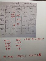
Hello... and thanks again for the persistent help!
Here is what I got:
Q32 2.9v across
Q14 pin 4:2.9. Pin 5: 2.5
R66 2.5 (both sides within about 0.2)
R65 2.5 (both sides within about 0.2)
R53 1.2/1.4
R49 1.2/0.54
Q3 pin 4: 0.54. Pin 5: 0.0
Strange that R49 and R66 measure the same value (180) in circuit, but the drop is so much more with R49.
Pin 5 also seems odd, so I rechecked with diode setting between pin 4 to pin 5 on both Q14 and Q3. Both showed the same result, ~0.5v.
Looks like two examples of different results despite same specs. Interesting.
Hi Peter,
I've attached a crude PDF showing your measurements and and also voltages I believe should appear at each node in the voltage divider chain.
A few entries are missing, as I wasn't sure how to interpret the R66 and R65 data. I estimate there should be about 0.4V across R66 and about 0.6V across R65, so I can't reconcile that with your data. I agree that voltage across R66 is especially peculiar.
One experiment might be to remove R66 and measure its resistance out-of-cicruit. Further, with R66 absent, you should be able to measure the remaining resistor values in situ, without stray paths affecting readings. With R66 absent, voltage should measure 0V at low side of the R66 site and nearly 2.9V on the high side of the R66 site.
Good luck. TTYL
Attachments
Here are the missing measurements.
Strange situation with R66. No short between the two pads and the resistor measures fine, yet no voltage drop.
The last R66 pads measurements were 2.66V, but I just just turned it in so maybe it hasn't settled yet.
Strange situation with R66. No short between the two pads and the resistor measures fine, yet no voltage drop.
The last R66 pads measurements were 2.66V, but I just just turned it in so maybe it hasn't settled yet.
Attachments
I’m not sure what to make of your last post. The starred note at bottom suggests that you cleared a short, as the pad voltages imply 2.6V across R66?
I was going to speculate that there was a short between the top pad of R66 and bottom of R65; that would yield 0V across R66 and R65, yet present resistance across the R66 terminals. If the short has been cleared, all resistor pads should present 0V with the exception of top pad of R66. Further, with R66 absent, you should be able to measure the resistors in circuit to confirm value and connections.
When replacing R66, I recommend cleaning pads with solder wick and using solder sparingly to avoid shorts.
Hello. Sorry for not being clear.
The R66 pads don't show a short. 0V on one pad, 2.6V on the other.
The R66 pads don't show a short. 0V on one pad, 2.6V on the other.
So the situation has improved re the post 95? I.e you somehow cleared a faulty path?
If so, and all resistor measurements look ok, restore R66 and check for appropriate voltage drops along the divider string. Also while transistors are still absent, check R52 resistance since it will still be isolated and easy to test.
Then install Q10 and confirm resistor network doesn’t change; then Q32 and no change. Finally, install Q8 and remove the four-diode clamp. With luck, the bias spreader should now behave and should respond to R53 adjustment. Return pot to minimum spreader voltage before reconnecting output stage.
Good luck!
- Home
- Amplifiers
- Solid State
- Help!!! Dumb-a$$ ham first mistake content