R12 could be replaced with a BJT, emitter to collector of Q1, collector to collector/base of Q6, and base to gnd; a common base cascode.🙂
 , and remove C3 at the same time since it's not doing anything useful.
As is, R12 is completely screwing everything up - it's dropping the full rail voltage, leaving Q1 saturated.
I suppose the intention was for R12 to drop half the supply voltage, leaving Q1's collector approx at ground potential. If so, it needs to be much lower resistance. CBS's way is better though.
Thanks CBS, to me it seems this circuit is arranged such that there is no ground referenced voltage divider for the AC feedback? I would have imagined there need be a resistor to ground from the two bases of the input devices.
I also see in my latest circuit, that I believe the second diff is assymetrical due to feedback coming into Q3 pumping lots of current through Q3 and hence into q1 base, and I do not have the other phase feedback present to balance this in the second diff (saturation aside). Comments on this?
I will work on your circuit tonight - did you make it or find it elsewhere? I appreciate your patience with me.
Godfrey: Thanks for your suggestions, yes I didn't put any thought into the output devices, I just threw them in to get the sim working quickly. I have read that laterals and verticals have different compensation requirements. I also have never worked with mosfets, but have touched on them lightly in my course. I have put the common base cascode in place now and I am playing with this.
Last edited:
Sorry I left out that the input source is a current source, ref to gnd not a voltage source. If you use input capacitors for both the +Vin and -Vin, there would be a resistor to GND to give a DC reference to the bases of the IPS and set the input LP filter Fc. However, if they are tied to 0V, the outputs would likely be offset a bit. This would be the summing node of the DC servo(s) input. I figured you could try a sim and see if it works in a more balanced way.
I don't have it now, long to the dustbin of history but I made a circuit somewhat similar to this, if I remember correctly , long ago as a learning bit to the project I'm working on now.🙂
I don't have it now, long to the dustbin of history but I made a circuit somewhat similar to this, if I remember correctly
, long ago as a learning bit to the project I'm working on now.🙂Okay CBS, I had a play with your circuit for a good few hours last night. I managed to get some alright looking results for a while, but I messed this up with further experimentation.
This morning I played with my original circuit some more, and I think it is converging on acceptable (as a proof of concept, and given appropriate output devices are used, and possibly lower V rails, will not demonstrate at full power, restricted to maybe +/-30v, 5A supplies).
Here are the figures:


FOURIER COMPONENTS OF TRANSIENT RESPONSE V(R_R243)
DC COMPONENT = 2.166564E-01
HARMONIC FREQUENCY FOURIER NORMALIZED PHASE NORMALIZED
NO (HZ) COMPONENT COMPONENT (DEG) PHASE (DEG)
1 1.000E+03 3.559E+01 1.000E+00 -1.798E+02 0.000E+00
2 2.000E+03 5.642E-03 1.585E-04 8.954E+01 4.492E+02
3 3.000E+03 7.371E-04 2.071E-05 -1.533E+02 3.862E+02
4 4.000E+03 3.104E-04 8.721E-06 -6.641E+01 6.529E+02
5 5.000E+03 1.774E-04 4.983E-06 -6.408E+01 8.350E+02
6 6.000E+03 1.680E-04 4.721E-06 -7.471E+01 1.004E+03
7 7.000E+03 1.766E-04 4.963E-06 -7.997E+01 1.179E+03
8 8.000E+03 1.691E-04 4.752E-06 -7.296E+01 1.366E+03
9 9.000E+03 2.041E-04 5.733E-06 -8.388E+01 1.534E+03
10 1.000E+04 1.863E-04 5.235E-06 -8.040E+01 1.718E+03
TOTAL HARMONIC DISTORTION = 1.605782E-02 PERCENT
I know it's not a good performer, it's just for the sake of a demonstration only (and to show some knowledge of measurement, test and simulation techniques). Basically to entertain the people assessing me, as opposed to me simply reeling off all the research and prior art I've looked at. Would also be a good benchmark for them to see, if/when I do design a fully differential amplifier, that it may perform better.
This morning I played with my original circuit some more, and I think it is converging on acceptable (as a proof of concept, and given appropriate output devices are used, and possibly lower V rails, will not demonstrate at full power, restricted to maybe +/-30v, 5A supplies).
Here are the figures:
FOURIER COMPONENTS OF TRANSIENT RESPONSE V(R_R243)
DC COMPONENT = 2.166564E-01
HARMONIC FREQUENCY FOURIER NORMALIZED PHASE NORMALIZED
NO (HZ) COMPONENT COMPONENT (DEG) PHASE (DEG)
1 1.000E+03 3.559E+01 1.000E+00 -1.798E+02 0.000E+00
2 2.000E+03 5.642E-03 1.585E-04 8.954E+01 4.492E+02
3 3.000E+03 7.371E-04 2.071E-05 -1.533E+02 3.862E+02
4 4.000E+03 3.104E-04 8.721E-06 -6.641E+01 6.529E+02
5 5.000E+03 1.774E-04 4.983E-06 -6.408E+01 8.350E+02
6 6.000E+03 1.680E-04 4.721E-06 -7.471E+01 1.004E+03
7 7.000E+03 1.766E-04 4.963E-06 -7.997E+01 1.179E+03
8 8.000E+03 1.691E-04 4.752E-06 -7.296E+01 1.366E+03
9 9.000E+03 2.041E-04 5.733E-06 -8.388E+01 1.534E+03
10 1.000E+04 1.863E-04 5.235E-06 -8.040E+01 1.718E+03
TOTAL HARMONIC DISTORTION = 1.605782E-02 PERCENT
I know it's not a good performer, it's just for the sake of a demonstration only (and to show some knowledge of measurement, test and simulation techniques). Basically to entertain the people assessing me, as opposed to me simply reeling off all the research and prior art I've looked at. Would also be a good benchmark for them to see, if/when I do design a fully differential amplifier, that it may perform better.
The output stage is not working properly, there should be about 150mA bias not 3A. You should see 33mV across R241 & R242. Reduce the value of R232 and place a pot in series. Vgs threshold of the outputs is about 3.5-4V for each, so the gate Vdc spread should be 7-8V. Figure Ohm's Law...
If you intend to use +/-30V, you should design the circuit for such voltages. If you intend to make a balanced amp, remember you get Vp=2 X Vcc. (Hint) If you are building a power supply, 25V caps are cheaper and smaller than 35V caps for the same uf's. +/-24V can supply 42Vp (figure in some Xformer sag) signal to the load with balanced output.
One more neat thing about balanced topology is you can use a single ended power supply and no output cap.🙂
I didn't have the pot because I still needed to manual enter values anyway (in orcad capture); however I see the advantage of having two resistors, that I can try to zero between them. What do you think about this arrangement. The bias conditions are as close to even as I can get them! But all looks good in DC and also for the output signals. Source resistors are dropping 47.5mV for the lower one, and 47.13mV for the upper one.

Just for this prototype, I will use a lab power supply but I appreciate your sound advice on power supply design. Are there any serious problems in this circuit layout why I shouldn't contruct it for a quick demo? I am yet to double check the datasheet of the FETs in the simulation to make sure they are appropriate but I will do this once I know the topology is sound. Is using veroboard likely to cause instability in the amplifier? I have not calculated phase margin, or the feedback in freq domain, but I assume it would be unconditionally stable and if so, veroboard shouldn't matter.
As for compensation, I need a Vbe or Vgs multiplier bias spreader on the heatsink to create the spread? I'll check my text books and add this in.
Last edited:
Yes, the Vgs multiplier is required if you intend on having a stable bias.
If it is unconditionally stable veroboard doesn't matter. Here is where I built the veroboard version of my balanced output amp. This one was unconditionally stable and I used it for over 1year before scraping it for parts, namely those THAT matched arrays... they're about $8 each.😱
There are some details you need to know if you intend on building this circuit with real parts. The output mosfets MUST have gate-source protection Zener diodes between G and S pins, as close to the device body as possible. Simulation doesn't show you the metal oxide shoot-through (and thus destruction) of the transistor when Vgs >+/-20V. This can happen if you have an instability or oscillation burst (which can happen under peak load current if the mosfet local frequency compensation is not adequate.)
Although this article does not apply exactly to what you are doing here, it is an interesting read. Pages 3-9 is relevent.
.......but I assume it would be unconditionally stable and if so, veroboard shouldn't matter.
If it is unconditionally stable veroboard doesn't matter. Here is where I built the veroboard version of my balanced output amp. This one was unconditionally stable and I used it for over 1year before scraping it for parts, namely those THAT matched arrays... they're about $8 each.😱
There are some details you need to know if you intend on building this circuit with real parts. The output mosfets MUST have gate-source protection Zener diodes between G and S pins, as close to the device body as possible. Simulation doesn't show you the metal oxide shoot-through (and thus destruction) of the transistor when Vgs >+/-20V. This can happen if you have an instability or oscillation burst (which can happen under peak load current if the mosfet local frequency compensation is not adequate.)
Although this article does not apply exactly to what you are doing here, it is an interesting read. Pages 3-9 is relevent.
Thank you CBS, yes I already purchased and read (several times) Bob's article, as I did not know it was available free on his website. It is in fact very helpful.
I have seen the protection diodes in place before and will be sure to implement these. Perhaps just soldering them directly across the mosfets pins would be the best move for verobaord.
I will update when I have included a Vgs multiplier, diode protection, and some realistic MOSFET device choices.
Then it will be veroboard and breadboard construction time!
Thanks for all the help mate, truly appreciated!
Symmetry
@ hpt
Hi, you might be interested in the Symmetry in this.
If i remember correctly it followed on to the next issue or 2, with later discussions etc.
Tried to find a PDF for you but wasn't able to locate it 🙁 I have the original issues, but not with me here.
If you find a good link please share it 🙂
Regards
@ hpt
Hi, you might be interested in the Symmetry in this.
Erno Borbely, High power high quality amplifier using mosfets, Wireless World, March 1983
If i remember correctly it followed on to the next issue or 2, with later discussions etc.
Tried to find a PDF for you but wasn't able to locate it 🙁 I have the original issues, but not with me here.
If you find a good link please share it 🙂
Regards
Thank you Zero D, I am trying to locate the articles. It is a shame that Borbelly has taken down his website, and it seems (relatively recent) wireless world articles are hard to find.
Hi hpt
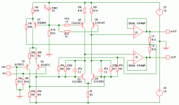
When you convert to balanced input with bridged output, the circuit can get a lot more complicated, but it doesn't have to. I'd vote for the simple option - just driving the 2 output stages from the 2 outputs of the second differential pair.
I simulated the circuit below and was pleasantly surprised at the results - distortion is only about 0.03% at 40V pk-pk output per side, as is, with no global feedback and using op-amps as dummy output stages. Final distortion will depend on your output stage and the amount of global feedback.
Looking at the components around the 2'nd diff pair, R6 and R7 set the voltage gain to 60dB and C1 and C2 roll off the open-loop response above about 15 KHz. With 30dB global feedback, the result would be 30dB gain and response to about 500KHz. btw, the circuit shown is fast enough to give full output to about 400KHz without slew rate limiting.
A heavy dose of common-mode feedback is applied via R12, R13, R8, R9 and R20 to keep the midpoint of the outputs at earth potential. I took this feedback down to the bases of Q3 and Q4 as well as up to the emitter of Q7 so the output stays centered if the supply voltage changes.
Anyway, good luck with the breadboarding.
Cheers - Godfrey
Attachments
Wow, thanks Godfrey, that is great advice you have given me and a good circuit. This is something like I had envisaged with my original explorations, in page one of this thread. I think for a simple solution this is great, and more within my means than looking at something as complex as a mirrored version of the circuit in Bob Cordells AES paper. Although a 'balanced current mirror' (see Cordells paper) driving the second differential may still be a good improvement?
I wonder how I might be able to demonstrate pulling two outputs from the second differential of my most recent circuit and use opamps as dummy output stages in the breadboard prototype. I suppose I must redesign the current sources to run off a lower voltage which the opamps can deal with like +/-15v or less. Also I must ensure the opamps can source/sink enough current through a dummy load at the rail voltages. Will investigate...
I wonder how I might be able to demonstrate pulling two outputs from the second differential of my most recent circuit and use opamps as dummy output stages in the breadboard prototype. I suppose I must redesign the current sources to run off a lower voltage which the opamps can deal with like +/-15v or less. Also I must ensure the opamps can source/sink enough current through a dummy load at the rail voltages. Will investigate...
No worries, the circuit as is works just fine on +-15V. Those current sources are actually pretty good. Hot tip: Ordinary, cheap LEDs make excellent low noise voltage references (better than zeners).I suppose I must redesign the current sources to run off a lower voltage which the opamps can deal with like +/-15v or less...
Using them in current sources like that also appeals to the lazy in me because it makes the arithmetic so easy. The voltage across the LED is about 1.7V and the transistor drops about 0.7V, so there's almost exactly 1V across the resistor. In the 2'nd stage I wanted 10mA, so I used 100R (1 volt / 10 mA = 100R). It's so simple you hardly have to think about it, let alone reach for a calculator.
For fun, I just tried a few different values of supply voltage without changing anything else in the circuit, to see the variation in DC output voltage. Results:
+-15V: +370mV
+-25V: -70mV
+-35V: -10mV
+-45V: +300mV
No real surprise, I suppose, since I fiddled with the value of R20 to get the least variation between supplies of +-25V and +-30V, but it's interesting to see the curve.
I haven't seen Bob's paper, but found the circuit in post 6 of this thread. I'm not sure if it's worth the extra complexity, but agree it should improve performance especially by drastically lowering the output impedance. Anyway, it does look interesting. Maybe I'll play with that a bit later.🙂... a 'balanced current mirror' (see Cordells paper) driving the second differential may still be a good improvement?
Well, for demo purposes I suppose it doesn't have to drive 8 ohms, but should at least be able to drive it's own feedback network etc plus maybe a dummy load of 1K or whatever.Also I must ensure the opamps can source/sink enough current through a dummy load at the rail voltages.
Well, for demo purposes I suppose it doesn't have to drive 8 ohms, but should at least be able to drive it's own feedback network etc plus maybe a dummy load of 1K or whatever.
Yes, I was thinking that. Out of the handful of opamps I checked, the best was about 120mA max output current. So if I were using 15 volt rails (or indeed less), I would still need a bigger than 8ohm load for the demo.
I was thinking to use my double differential circuit which was shown with the mosfet output stage, but in the opamp demo fashion.
Should provide a quick and dirty way of demonstrating two cascaded LTPs 🙂 People are probably scoffing at me for wanting to show such a basic thing, but it is merely complementing a presentation regarding my research and learning etc. and where I want to take my design. It is just for entertainment purposes really, and to show that at least a basic part of my design is physically viable at this point through the year.
Yes, it is a nice, simple and effective current source.
I will post up how the demo and presentation goes in about a weeks time. Thanks for your help 🙂
Hi
For a 1K load, a simple CCS loaded class A follower should suffice I would think. With +/-25V, 300mA bias should be more than enough, it would be simpler than an op-amp and could run with +/-25V. Godfrey's circuit in post 31 is interesting, it looks like one of the early 'proto' circuits I played with back when I stumbled on this crazy idea of balanced outputs for Hi-Fi. In my experience not using very closely matched components may create a DC offset, at least between the two outputs. Perhaps you could sim the circuit with slightly mis-matched transistors, as would be in the real world, that is if you did not put much effort into the matching process. Although implemented differently than in my balanced output amp, it uses common mode feedback to balanced the VAS current bias via modulation of the common mode current source for the input diff. It looks to me that if there is not good matching between Q's 1&2, 3&4, and a relativity low FB factor, a balance might be struck where one of the outputs is offset pos and the other offset neg, resulting in a solution to the CMFB loop but not the differential loops. It would be interesting how this circuit might work with a THAT300 series matched array employed. I never used these when I was working on a similar circuit, I had none on hand. Only problem (other than their cost😱 ) is they are 40Vceo so the VAS would have to be cascode or lower Vcc to +/-20V. There are other matched arrays out there that might be cheaper.
For a 1K load, a simple CCS loaded class A follower should suffice I would think. With +/-25V, 300mA bias should be more than enough, it would be simpler than an op-amp and could run with +/-25V. Godfrey's circuit in post 31 is interesting, it looks like one of the early 'proto' circuits I played with back when I stumbled on this crazy idea of balanced outputs for Hi-Fi. In my experience not using very closely matched components may create a DC offset, at least between the two outputs. Perhaps you could sim the circuit with slightly mis-matched transistors, as would be in the real world, that is if you did not put much effort into the matching process. Although implemented differently than in my balanced output amp, it uses common mode feedback to balanced the VAS current bias via modulation of the common mode current source for the input diff. It looks to me that if there is not good matching between Q's 1&2, 3&4, and a relativity low FB factor, a balance might be struck where one of the outputs is offset pos and the other offset neg, resulting in a solution to the CMFB loop but not the differential loops. It would be interesting how this circuit might work with a THAT300 series matched array employed. I never used these when I was working on a similar circuit, I had none on hand. Only problem (other than their cost😱 ) is they are 40Vceo so the VAS would have to be cascode or lower Vcc to +/-20V.
There are other matched arrays out there that might be cheaper.
Last edited:
Very interesting CBS!
So in terms of advantages for a fully differential 'balanced' amplifier, bridging a load: (tell me if I am wrong)
CMRR
PSRR
Ground noise and
ground loop immunity
Double output swing for given rails
double (increased) slew rate (i think?)
half the loading seen by (each 'half') the amplifier, but lower damping factor as a result? (can still be accounted for)
Disadavantages:
essentially double the component count
strong reliance on matched components
possibly complicated feedback requirements
Very interesting CBS!
So in terms of advantages for a fully differential 'balanced' amplifier, bridging a load: (tell me if I am wrong)
1) CMRR
2) PSRR
3) Ground noise and ground loop immunity
4) Double output swing for given rails
5) double (increased) slew rate (i think?)
6) half the loading seen by (each 'half') the amplifier, but lower damping factor as a result? (can still be accounted for)
Disadavantages:
7) essentially double the component count
8) strong reliance on matched components
9) possibly complicated feedback requirements
1) yes
2) yes
3) yes, but conditional, layout critical.
4) yes, but remember you have essentially full wave rectified signal current flowing from each rail, not half as in single end output amps. This means you need twice the filter capacitor uf's compared to single end amp PS.
5) yes, SR is the sum of both output phases
6) yes, because the output is full bridge instead of half bridge, think of SMPS transformer drive topology. But damping factor is more determained by the output Z and other circuit topology such as feedback or feedforward.
7) essintially, but not much more than Bob's diferential VAS amplifier.
8) For best results, matched components should be used IMO.
9) Yes, compensation and layout is important as well.
.
Last edited:
- Status
- Not open for further replies.
- Home
- Amplifiers
- Solid State
- Help designing double differential symmetrical amp