Hi everybody,
I am a EE undergraduate, relatively new to audio amp design. I am working on a design involving an LTP input stage, LTP voltage amp stage, and two opposite symmetrical class-AB push-pull output stages driving a load in a bridged fashion. Essentially there are two signal paths, one of each opposite phase. Of course the input would be driven by a balanced signal.
This will be something kind of similar to the early 1980's hitachi designs. I may later consider implementing a JFET input stage, to keep the DC offset in check. I haven't thought too much about OPS dveices yet, but maybe MOSFETS maybe BJTs.
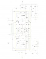
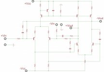
Here is where my design is currently and the time domain simulation (please note the output signal trace is divided by 1000):


Please, I would highly appreciate any advice, criticism, suggestions on how to move ahead, etc. Yes, I am aware that this circuit is probably far from optimised. I don't doubt that it may be entirely ill-concieved (I hope not). I have yet to do the maths properly, have just done some rough napkin calcs. Probably I will solidify the emitter degen values, and the current mirrors, design some proper ccs, once I figure out how to apply feedback to this thing? And DC feedback also. DC servo maybe?
I am working with Self, Slone and Cordells fantastic books, but the design I wish to do seems somewhat unconventional with respect to what is covered in these books. I believe for a newbie like me, it would have been much easier to work thorugh a simple 3-stage design, but unfortunately I must work with what I have shown you so far.
I have checked out Linsley-Hoods book, and this gave some good reference to the Hitachi application manual which I have now managed to download and investigate. Also I believe Duncan's book has some good examples of these 80's Hitachi amps, I haven't checked this out yet but I am in the rocess of getting it.
If anybody has copies of the 1981 Hitachi manual I am tlaking about, please let me know, I'd love to see more pages of these!
Regards,
hpt
I am a EE undergraduate, relatively new to audio amp design. I am working on a design involving an LTP input stage, LTP voltage amp stage, and two opposite symmetrical class-AB push-pull output stages driving a load in a bridged fashion. Essentially there are two signal paths, one of each opposite phase. Of course the input would be driven by a balanced signal.
This will be something kind of similar to the early 1980's hitachi designs. I may later consider implementing a JFET input stage, to keep the DC offset in check. I haven't thought too much about OPS dveices yet, but maybe MOSFETS maybe BJTs.
Here is where my design is currently and the time domain simulation (please note the output signal trace is divided by 1000):
Please, I would highly appreciate any advice, criticism, suggestions on how to move ahead, etc. Yes, I am aware that this circuit is probably far from optimised. I don't doubt that it may be entirely ill-concieved (I hope not). I have yet to do the maths properly, have just done some rough napkin calcs. Probably I will solidify the emitter degen values, and the current mirrors, design some proper ccs, once I figure out how to apply feedback to this thing? And DC feedback also. DC servo maybe?
I am working with Self, Slone and Cordells fantastic books, but the design I wish to do seems somewhat unconventional with respect to what is covered in these books. I believe for a newbie like me, it would have been much easier to work thorugh a simple 3-stage design, but unfortunately I must work with what I have shown you so far.
I have checked out Linsley-Hoods book, and this gave some good reference to the Hitachi application manual which I have now managed to download and investigate. Also I believe Duncan's book has some good examples of these 80's Hitachi amps, I haven't checked this out yet but I am in the rocess of getting it.
If anybody has copies of the 1981 Hitachi manual I am tlaking about, please let me know, I'd love to see more pages of these!
Regards,
hpt
You can't take a differential output from a normal current mirror, as the input and output sides have completely different impedances and DC voltages.
Personally I have never seen the point of fully differential designs, as the complications outweigh any small advantages, but that is a discussion for another day.
Personally I have never seen the point of fully differential designs, as the complications outweigh any small advantages, but that is a discussion for another day.
avoid true complementary output designs like the hitachi applications with 2SK135/2SJ49 and that one listed about
http://www.diyaudio.com/forums/soli...l-mosfets-class-ab-overview-p-spice-urls.html
a good approach offer this thread:
http://www.diyaudio.com/forums/solid-state/56833-nvmos-amplifier-30.html
especially post 297
more ideas I have listed there:
http://www.diyaudio.com/forums/soli...better-audio-non-complements-audio-power.html
Have you tried a bridge topology, iow complementary cascade differential circuit? Having both phase VAS outputs operating in complementary push pull has some advantages.🙂 As far as the above schematic, 600mA could not be flowing for 2Ivas source, 300mA X 1K is 300V...not enough room. 2Ivas current is actually zero. Current could not flow to the bases of 2Q1/2Q2 because 2Q10/2Q11 has no base current DC bias and do not conduct, thus are merely open circuits. Jumping into linear audio amp design and starting with balanced topology may not be the best place to start. Even if this was to be typical LIN, there are several fundamental issues to be worked out in the above diagram.
Full complementary balanced topology works very well, but it has to be implemented properly.
I added a drawing of the VAS stage in this amp. The complementary cascade diff is outlined in yellow, along with all the wonderful cascode connections. The feedback type CCS or ring CCS is for the bias currents, in this case active, but they can be static by replacing the CCS circuits with resistors and removing the common mode loops.
Even if this was to be typical LIN, there are several fundamental issues to be worked out in the above diagram.Full complementary balanced topology works very well, but it has to be implemented properly.
I added a drawing of the VAS stage in this amp. The complementary cascade diff is outlined in yellow, along with all the wonderful cascode connections.
The feedback type CCS or ring CCS is for the bias currents, in this case active, but they can be static by replacing the CCS circuits with resistors and removing the common mode loops.Attachments
Last edited:
Thanks CBS240. I realise I am jumping in the deep end with this kind of design, but unfortunately I am required to produce in some way a balanced or bridged design, and preferably with a differential VAS with two opposite phase signal paths. I also realise that many people believe there is no point of fully differential designs.
I was very suspicious of the normal current mirror on the LTP taking both phases, as it would try to force equal currents in both legs, but I tried it and it actually seemed to work okay in SPICE. Obviously I can't be taking things at face value and this was a silly idea.
So I will analyse what you have told me regarding the problems in my above circuit, and hopefully this will teach me some more things about such a design.
The problem is, I am referencing schematics in the Hitachi application notes, as well as a few wodd balls in Self and Slone, and then trying to apply the design methodology from Self, Slone and Cordell regarding a 3-stage Lin.
" Having both phase VAS outputs operating in complementary push pull has some advantages." Please elaborate on this point. 🙂
Please if you could suggest any references where I might find information regarding the design of thiskind of amplifier, this would be great. I originally wanted to steer clear of complementary differential as this looks even more complicated to me. But I will be looking through the amp you showed me.
Cheers
EDIT: Something like the front-end of the Kaneda amplifier http://www.bonavolta.ch/hobby/en/audio/kaneda_p.htm coupled to two output stages one for each phase, and driving the load bridged. Compared to a non-bridged scenario, should have better slew rate, less demand on power rails, and less load on amplifier output, no?
Last edited:
Thanks jcx. I have read that part of the book; however after buying and digesting the AES paper, the amp makes a lot more sense. This is a great reference.
I now further realise how misguided my own attempt was at the circuit shown, lacking proper biasing, the mirror, the vas collector load resistors / ccs current and lack of rail headroom, and all. I guess I can't forget basic circuit theory when I am plodding through optimisations on example circuits and what not.
Now I am wondering how this amp might be implemented with a) balanced input, and b) differential output / bridge output.
you could load each side of the 2nd "VAS" diff pair with CCS for phase split drive but balancing the CCS current sum against the diff pair tail current may require a servo
or you could duplicate the whole 2nd diff pair/mirror VAS and connect it anti-phase to Bob's Q8,9
differential out amps need something setting/controling the common mode of the output - see the lit on recent diff in/out op amps - they have a common mode pin and internal servo subcircuit
or you could duplicate the whole 2nd diff pair/mirror VAS and connect it anti-phase to Bob's Q8,9
differential out amps need something setting/controling the common mode of the output - see the lit on recent diff in/out op amps - they have a common mode pin and internal servo subcircuit
" Having both phase VAS outputs operating in complementary push pull has some advantages." Please elaborate on this point. 🙂
Better symmetrical slewing. Since your output is the difference between the two phases, then having a distortion in the negative phase will not be canceled by the same distortion in the positive phase, so you end up with the distortion in both halves of the signal, as far as the load sees.
A symmetrical common mode distortion will not show up at the load with BAL outputs. Your double differential is a good approach, try building the same circuit with opposite polarity devices and put them together. Symmetry between phases and symmetry between polarity of devices.🙂 Think of building two complementary amplifiers, mirror images of each other reflected over the common mode biasing points, one side of the differentials' for pos phase and the other for neg phase, together with the same common mode bias currents.
differential out amps need something setting/controling the common mode of the output - see the lit on recent diff in/out op amps - they have a common mode pin and internal servo subcircuit
This is a good point. There must be a DC reference for the inputs that bias the DC output of each phase to zero volts. You should have no offset between each phase and gnd, this ensures no offset between the two outputs and that they have equal dynamic range.
Last edited:
Here is where my design is currently and the time domain simulation (please note the output signal trace is divided by 1000):
You might like to rearrange it, to get the working balanced circuit:
But 1k resistors and 600mA CCS is impossible. You would get it saturated.
Attachments
Last edited:
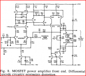
Okay, I have put Cordell's entire front end from the AES Mosfet Amp article into PSPICE to help me understand the operation.
The bias voltages and currents all look symmetrical and account for all the Vbe drops etc. When I run time domain simulation, I get "soft" clipping (I think 'softened' due to the back to back protection diode action) upstream of the first set of BJT cascodes to the jfet input LTP. This obviously continues all the way through to the input of the final 'darlington cascode current mirror' loading the second 'VAS' LTP. On the output of this current mirror, ie. where the signal is taken spread across 22v difference, to the output stage, I just get the square waves shown.
Would this simply be because I have not made the complete circuit, and it is lacking global feedback? Because I see that it has compensated feedback none-the-less. Or have I stuffed something else up...
I am going to keep working on my original circuit concept, using the cordell reference for some guidance. Will worry about balanced/mirror/complementary etc issues after I have something basic, single-ended working. Thank you all for your patience with me!
Last edited:
Without a closed loop, the feedback, the gain set is the open loop gain. OL gain varies with frequency but at AF the OLG is very high so you are simply overdriving the amp.
Okay cool, thank you. I thought the feedback from positive output side would control the gain somewhat, but I see the voltage divider is only a multiplying factor of 0.25, and with the series cap presenting lower impedance at higher frequencies.
Quote JCK:
"you could load each side of the 2nd "VAS" diff pair with CCS for phase split drive but balancing the CCS current sum against the diff pair tail current may require a servo
or you could duplicate the whole 2nd diff pair/mirror VAS and connect it anti-phase to Bob's Q8,9
differential out amps need something setting/controling the common mode of the output - see the lit on recent diff in/out op amps - they have a common mode pin and internal servo subcircuit"
These both seem like good ideas to me.
This appeals to me because I would like to create differential signal paths all the way through the amp, before (or without) contemplating complementary symmetry.
Okay, gone back to the drawing board. Learned a few things (thanks guys). I may still have misunderstanding, please do tell me!
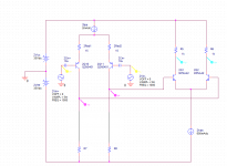
Original schematic with biasing shown:

My modifications so far:

Adjusted the bias pot to balance the output mosfets (please tell me if I have misunderstood this point):

Output for a 500mV input (after adjusting feedback ratio):

And finally, distortion at the same output amplitude as previous graph, at 1Khz:

According to the output file:
FOURIER COMPONENTS OF TRANSIENT RESPONSE V(N06700) MODIFIED AMPLIFIER
DC COMPONENT = -5.420615E-01
HARMONIC FREQUENCY FOURIER NORMALIZED PHASE NORMALIZED
NO (HZ) COMPONENT COMPONENT (DEG) PHASE (DEG)
1 1.000E+03 2.768E+01 1.000E+00 1.949E+00 0.000E+00
2 2.000E+03 2.082E-03 7.522E-05 -8.380E+01 -8.770E+01
3 3.000E+03 3.680E-04 1.329E-05 9.471E+00 3.623E+00
4 4.000E+03 2.324E-04 8.397E-06 1.074E+02 9.959E+01
5 5.000E+03 1.536E-04 5.548E-06 9.228E+01 8.253E+01
6 6.000E+03 1.597E-04 5.768E-06 3.358E+01 2.189E+01
7 7.000E+03 1.505E-04 5.435E-06 7.324E+01 5.960E+01
8 8.000E+03 2.033E-04 7.345E-06 1.386E+02 1.230E+02
9 9.000E+03 1.825E-04 6.593E-06 1.064E+02 8.888E+01
10 1.000E+04 2.745E-04 9.917E-06 6.072E+01 4.123E+01
TOTAL HARMONIC DISTORTION = 7.870971E-03 PERCENT
Which is an improvement on th eoriginal unmodified amplifier which was:
FOURIER COMPONENTS OF TRANSIENT RESPONSE V(N06700) ORIGINAL AMPLIFIER
DC COMPONENT = -5.529513E-01
HARMONIC FREQUENCY FOURIER NORMALIZED PHASE NORMALIZED
NO (HZ) COMPONENT COMPONENT (DEG) PHASE (DEG)
1 1.000E+03 2.770E+01 1.000E+00 -2.103E-01 0.000E+00
2 2.000E+03 3.259E-02 1.176E-03 9.375E+01 9.417E+01
3 3.000E+03 3.475E-02 1.254E-03 9.156E+01 9.219E+01
4 4.000E+03 3.470E-02 1.253E-03 9.147E+01 9.232E+01
5 5.000E+03 3.464E-02 1.250E-03 9.125E+01 9.230E+01
6 6.000E+03 3.471E-02 1.253E-03 9.082E+01 9.208E+01
7 7.000E+03 3.471E-02 1.253E-03 9.075E+01 9.223E+01
8 8.000E+03 3.466E-02 1.251E-03 9.066E+01 9.234E+01
9 9.000E+03 3.460E-02 1.249E-03 9.060E+01 9.249E+01
10 1.000E+04 3.472E-02 1.253E-03 9.047E+01 9.257E+01
TOTAL HARMONIC DISTORTION = 3.731724E-01 PERCENT
So how come my +ve and -ve gain is not symmetrical, even though there is nearly 0 dc offset? Is it variation in the physical properties of the output mosfets? I can't get rid of it no matter how much I tweak!
My next step will be to go through and perform the emitter degeneration calculations, implement a real current source, and perhaps improved mirror (helper transistor), calculate the bias properly. I will need more appropriate output devices if this were to be realised. Re-assess the rail voltage for power and current handling at the output (and practical temperature control). Calculate the miller compensation. I do not think there needs to be two miller caps, only one on the negative output of the first LTP.
After this, I will knock up a low power prototype to demonstrate the concept (run off bench power supply). I was going to make a PCB, but will veroboard be okay for a low power prototype as described?
Then I will investigate mirroring this topology, which will present difficulties with providing feedback. Because if I have the feedback divider resistor, and dc blockign cap (for 100% dc feedback), does that mean the BJTs can still draw sufficient bias current from the approx. 0v output line (through the load or from the output devices?)? Or do I need to control the DC feedback another way? That is, if feedback is applied to both sides of the input LTP.
By the way, I also PSPICED a fully mirrored version of the cordell amplifier involving the second ltp being replicated in opposite phase off the dual emitter-followers. I rearranged the topology to be somewhat vertical.
At the moment, I really need to stay simpler unfortunately so that I can likely achieve good results more easily instead of possibly achieve no results from a complex circuit. Also I should learn more this way.
Please any advise or criticism is welcome. Cheers. hpt (by the way, this is part of a uni project involving research also)
Original schematic with biasing shown:
My modifications so far:
Adjusted the bias pot to balance the output mosfets (please tell me if I have misunderstood this point):
Output for a 500mV input (after adjusting feedback ratio):
And finally, distortion at the same output amplitude as previous graph, at 1Khz:
According to the output file:
FOURIER COMPONENTS OF TRANSIENT RESPONSE V(N06700) MODIFIED AMPLIFIER
DC COMPONENT = -5.420615E-01
HARMONIC FREQUENCY FOURIER NORMALIZED PHASE NORMALIZED
NO (HZ) COMPONENT COMPONENT (DEG) PHASE (DEG)
1 1.000E+03 2.768E+01 1.000E+00 1.949E+00 0.000E+00
2 2.000E+03 2.082E-03 7.522E-05 -8.380E+01 -8.770E+01
3 3.000E+03 3.680E-04 1.329E-05 9.471E+00 3.623E+00
4 4.000E+03 2.324E-04 8.397E-06 1.074E+02 9.959E+01
5 5.000E+03 1.536E-04 5.548E-06 9.228E+01 8.253E+01
6 6.000E+03 1.597E-04 5.768E-06 3.358E+01 2.189E+01
7 7.000E+03 1.505E-04 5.435E-06 7.324E+01 5.960E+01
8 8.000E+03 2.033E-04 7.345E-06 1.386E+02 1.230E+02
9 9.000E+03 1.825E-04 6.593E-06 1.064E+02 8.888E+01
10 1.000E+04 2.745E-04 9.917E-06 6.072E+01 4.123E+01
TOTAL HARMONIC DISTORTION = 7.870971E-03 PERCENT
Which is an improvement on th eoriginal unmodified amplifier which was:
FOURIER COMPONENTS OF TRANSIENT RESPONSE V(N06700) ORIGINAL AMPLIFIER
DC COMPONENT = -5.529513E-01
HARMONIC FREQUENCY FOURIER NORMALIZED PHASE NORMALIZED
NO (HZ) COMPONENT COMPONENT (DEG) PHASE (DEG)
1 1.000E+03 2.770E+01 1.000E+00 -2.103E-01 0.000E+00
2 2.000E+03 3.259E-02 1.176E-03 9.375E+01 9.417E+01
3 3.000E+03 3.475E-02 1.254E-03 9.156E+01 9.219E+01
4 4.000E+03 3.470E-02 1.253E-03 9.147E+01 9.232E+01
5 5.000E+03 3.464E-02 1.250E-03 9.125E+01 9.230E+01
6 6.000E+03 3.471E-02 1.253E-03 9.082E+01 9.208E+01
7 7.000E+03 3.471E-02 1.253E-03 9.075E+01 9.223E+01
8 8.000E+03 3.466E-02 1.251E-03 9.066E+01 9.234E+01
9 9.000E+03 3.460E-02 1.249E-03 9.060E+01 9.249E+01
10 1.000E+04 3.472E-02 1.253E-03 9.047E+01 9.257E+01
TOTAL HARMONIC DISTORTION = 3.731724E-01 PERCENT
So how come my +ve and -ve gain is not symmetrical, even though there is nearly 0 dc offset? Is it variation in the physical properties of the output mosfets? I can't get rid of it no matter how much I tweak!
My next step will be to go through and perform the emitter degeneration calculations, implement a real current source, and perhaps improved mirror (helper transistor), calculate the bias properly. I will need more appropriate output devices if this were to be realised. Re-assess the rail voltage for power and current handling at the output (and practical temperature control). Calculate the miller compensation. I do not think there needs to be two miller caps, only one on the negative output of the first LTP.
After this, I will knock up a low power prototype to demonstrate the concept (run off bench power supply). I was going to make a PCB, but will veroboard be okay for a low power prototype as described?
Then I will investigate mirroring this topology, which will present difficulties with providing feedback. Because if I have the feedback divider resistor, and dc blockign cap (for 100% dc feedback), does that mean the BJTs can still draw sufficient bias current from the approx. 0v output line (through the load or from the output devices?)? Or do I need to control the DC feedback another way? That is, if feedback is applied to both sides of the input LTP.
By the way, I also PSPICED a fully mirrored version of the cordell amplifier involving the second ltp being replicated in opposite phase off the dual emitter-followers. I rearranged the topology to be somewhat vertical.
At the moment, I really need to stay simpler unfortunately so that I can likely achieve good results more easily instead of possibly achieve no results from a complex circuit. Also I should learn more this way.
Please any advise or criticism is welcome. Cheers. hpt (by the way, this is part of a uni project involving research also)
By the way, the mosfet output stage was only used because it was the quickets easiest way to complete the design. I will put more design thought into this at a later stage. I just need to prove the double differential concept at this point in time.
Hi
Why is there 10V spread between the gates of the output devices? Id is 2.7A. You might as well include the source ballast resistors in the circuit, they will be needed with these devices, ~0R2. Emitter resistors if you use BJT outputs. There is no Vgs multiplier, these devices need compensation. This is a single ended signal amp. The other side of the VAS differential is a mirror not an output. There should be equal Vce across Q1 & Q2. Transistors operation in the linear region have temperature dependent variables, such as Vbe, Hfe, and Gm. The differential only works as such if both sides conduct the same current, thus the temperature will remain equal if the two transistors have equal Vce. If Q1 & Q2 are different temperatures, the DC offset will drift wrt time. R12 could be replaced with a BJT, emitter to collector of Q1, collector to collector/base of Q6, and base to gnd; a common base cascode.🙂
However I thought the intent here was to build a balanced amplifier.😕
Last edited:
Thankyou CBS,
"This is a single ended signal amp. The other side of the VAS differential is a mirror not an output."
"However I thought the intent here was to build a balanced amplifier."
--Yes I know this, I am just starting off with something simple as apparently I do not yet have enough experience or understanding to tackle the bigger problems just yet. So if I can get a single ended working, I can then alter the circuit as required to mirror it. IE replicate the second mirror-loaded LTP to the opposite phase of the input LTP or something like this. I also wish to have some basic concepts ready to demonstrate practically in a two weeks re. this project, as this would be better than merely trying to demonstrate my futile (up to this point) research. My goal is still to develop a differential amplifier though. This project will carry on throught the rest of the year. Hopefully bulk of design can be done this next 8 weeks or so, as I learn more about amp design.
" R12 could be replaced with a BJT, emitter to collector of Q1, collector to collector/base of Q6, and base to gnd; a common base cascode. "
--I have seen this done in many circuits. What are the advantages and disadvantages?
"Why is there 10V spread between the gates of the output devices?"
--I have no idea. Before I adjusted the resistor value between the two gate connections, there was a 7v spread. Neither spread is symmetrical. I do not know the theory regarding this spread, but I I could not help it by tweaking the circuit. What spread should there be? I'd have guessed this defines the voltage Q point?
"There is no Vgs multiplier, these devices need compensation."
--I don't understand, please explain this a bit further...
EDIT: I partly understand this point now, the design originally used lateral mosfets and these can have a resistor instead of a Vgs multiplier, but vertical mosfets need compensation due to their positive temeprature coefficient at normal bias currents. I am sure there are caveats to this.
Cheers,
hpt
Last edited:
In your latest circuit, changing the value of R14 changes the voltage between the gates of the Mosfets. This voltage determines the idling current through the Mosfets so it is important to get it right.
The gate threshold voltage can vary a lot from one Mosfet to the next so a trimpot should be used to allow for adjustment of the bias voltage.
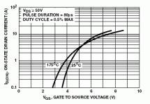
Then there's another problem - the required gate voltage changes with temperature (see pic below from the datasheet). That's the compensation CBS was talking about - temperature compensation. I haven't played with Mosfets so I'm not sure how that's normally sorted out with them.
Edit: I just saw your edit - sounds like you got the idea already.
btw: Your rail voltages (+-50V) are suitable for a really high powered amp, but the Mosfet's power rating isn't nearly high enough. I'd suggest looking at some other designs on the forum to get an idea of what type of Mosfet to use (and how many).
The gate threshold voltage can vary a lot from one Mosfet to the next so a trimpot should be used to allow for adjustment of the bias voltage.
Then there's another problem - the required gate voltage changes with temperature (see pic below from the datasheet). That's the compensation CBS was talking about - temperature compensation. I haven't played with Mosfets so I'm not sure how that's normally sorted out with them.
Edit: I just saw your edit - sounds like you got the idea already.
btw: Your rail voltages (+-50V) are suitable for a really high powered amp, but the Mosfet's power rating isn't nearly high enough. I'd suggest looking at some other designs on the forum to get an idea of what type of Mosfet to use (and how many).
Attachments
Last edited:
Mosfets are more forgiving than BJTs with regard to thermal bias stability because thier transconductance is much less around the bias point than BJTs and require larger variation in Vgs vs Id than Vbe vs Ic of BJT. Using a BJT for Q12 places a static voltage on the collector of Q1, -0.6V. This voltage should be close to that of the collector of Q2 so they maintain equal Vce. In your circuit, Vce of Q1 is 0.02V, so Q1 is saturated, it's not doing anything.
from previous post
....There should be equal Vce across Q1 & Q2. Transistors operating in the linear region have temperature dependent variables, such as Vbe, Hfe, and Gm. The differential only works as such if both sides conduct the same current, thus the temperature will remain equal if the two transistors have equal Vce. If Q1 & Q2 are different temperatures, the DC offset will drift wrt time....
- Status
- Not open for further replies.
- Home
- Amplifiers
- Solid State
- Help designing double differential symmetrical amp