Even the amp is designed with symetrical power supply, i would use cap on the output as safety first.
I would advise to use that cap on output as I mentioned, it prevents fireworks in the speaker.
Remember it must be bipolar, a regular electrolytic will explode when subject to high AC voltage.3000 to 4000 uF, appropriate voltage
The original circuit has other problems, such as not bootstrapped Vas load, which will needlessly waste output power.
Also not needed and excursion limiting 200 ohm resistor on driver transistor collectors.
+1 on straight using a properly designed circuit, suggested APEX or similar ones.
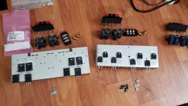
As of PCBs, even from Kenya you can order cheap and excellent Chinese PCBs (JLPCB comes to mind, but there are others) which will arrive by mail within a week.
You need certain PCB manufacturing files called Gerbers, they can´t work "just with images", but I am certain Apex (and probably others) have them available, just check the corresponding threads.
If not, learn and practice "laser toner transfer ironing" PCBs, many videos on that.
With some practice, quite good results.
I still use that method for quick prototypes, where I do not want to wait a week for each change.

Kenya may have high duties like Argentina...may be part of the reason he is not willing to import the parts.
JMFahey is right, use bipolar on the output. I typically create bipolar just by putting normal electrolytic caps back to back. You just have to use bigger value. See my thread 'what bjts for buffer'. Lots of pictures there. I was working of ClassA buffer, completely different goal, low power but pure classA sound without crossover distortion and no global feedback.
https://www.diyaudio.com/community/threads/direction-of-diodes-in-an-amplifier.379908/page-3
https://www.diyaudio.com/community/threads/output-bjts-for-buffer.386324/page-5
https://www.diyaudio.com/community/threads/direction-of-diodes-in-an-amplifier.379908/page-3
https://www.diyaudio.com/community/threads/output-bjts-for-buffer.386324/page-5
Attachments
Probably, but there is a "universal" Law or regulation, most probably embedded in the (worldwide) Postal Union , which typically allows:Kenya may have high duties like Argentina...may be part of the reason he is not willing to import the parts.
*a smallish allowance, under which no Tariff is charged.
Typically U$50 per Month, worst case U$ 25
* a maximum item count of 3 "because more than that is presumed Commercial resale, not Personal use"
That is used by everybody here to make small purchases, it definitely allows for 3 empty/unpopulated boards (which fit in a padded envelope) a Month.
Just last week I used it to buy a pocket oscilloscope from Alibaba (sorry wiseoldtech 😉 )
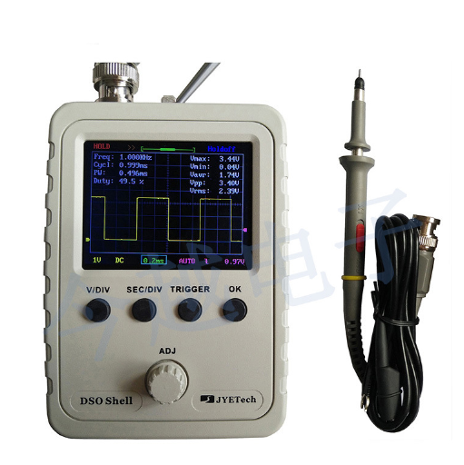
All of $20.50 for the product + 8.75 for cheapest Alicdn freight, it took almost 2 Months to arrive (by sea shipping container).
Dirt cheap, well within our U$50 allowance, I had to pick it up at the Postal/Custome office because X-Rays detected "electronics inside" and they had to visually check what I actually bought, but didn´t have to pay a cent for it, only U$2 "Postal Office processing fees" 🙄
Meaning, I bet something similar exists in Kenya.
EDIT: just checked, Kenya IS a full member, so I bet this small import type is allowed.
Check with your main postal office, a local one may have no clue about it.
https://www.upu.int/en/Universal-Postal-Union/About-UPU/Member-Countries?csid=-1&cid=164
Thanks for this,Use just one pair, the populated PCB are sold here in India.
Kenya, just check.
And as Adason says, there are plenty of circuits for that very popular transistor pair.
Search for "5200/1943 amp schematic",
Not to sound offensive or picky but ... From experience, tech guys from India and china love exaggerating figures (just watch any amp video on YouTube) . It becomes hard to follow. You see stuff like "1000watts super bass amplifier" and the circuit is just a couple resistors and a single pair of output bjts, all on a heat sink. I've also seen a thread here pointing out misaligned bias diodes on those schematics.
I however trust all of you here on this community 101% since y'all are real diehards and super enthusiasts
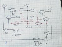
@Citizen124032 About the right half plane zero, at least when you look at the transimpedance with no load, model the transistor as an ideal voltage-controlled current source and the differential pair output as a current source, you indeed remove the emitter resistor from the equation when the other side of the current source is tied to the emitter.

Upper part: signal current Iin flows through the Miller compensation capacitor, collector, emitter and emitter resistor back to the source.
Signal voltage at the emitter: RE Iin
Signal voltage at the base: RE Iin + Iin/gm
Signal voltage at the collector: RE Iin + Iin/gm - Iin/(s CMiller)
Transfer function from the input current to the signal voltage at the collector:
RE + 1/gm - 1/(s CMiller) = ((RE + 1/gm) s CMiller - 1)/(s CMiller)
Numerator is zero at s = 1/((RE + 1/gm) CMiller)
Bottom part: signal current Iin flows through the Miller compensation capacitor, collector and emitter back to the source, but not through the emitter resistor.
Signal voltage at the emitter: 0
Signal voltage at the base: Iin/gm
Signal voltage at the collector: Iin/gm - Iin/(s CMiller)
Transfer function from the input current to the signal voltage at the collector:
1/gm - 1/(s CMiller) = ((1/gm) s CMiller - 1)/(s CMiller)
Numerator is zero at s = 1/((1/gm) CMiller)
Those are sales guys.
Even Philips put stickers saying 400W PMPO on sets with 2 x 20W chip amps....
And do not talk about Akai....2200W!
So if some seller does it, he is following an existing example.
In my world, PMPO is 2 x max. power into 8 ohms, RMS, for half an hour. That gives a pretty good idea of the heat sink, power supply and so on.
As you are a novice, it is better to start with a simple design, multiple transistors require matching and so on.
And you may be satisfied with the output.
Thanks MarcelvdG for supplying these equations.
You start with "model the transistor as an ideal voltage-controlled current source", but your reasoning is starting with "signal current Iin flows through"!
No problem, as this reasoning is clear enough. Hence my first remark "quasi-differential", where the tail of a differential stage is also left out of any equation.
Yes, because the transistor is modelled as a voltage-controlled current source, all the current has to go through the source part (collector) rather than the controlling part (base), which helps to keep the equations simple.
So the open loop gain increases considerable but is less linear compared with the classical 'Re-included' version. But which one is more stable (DC, temperature) given the tropical location in Kenya?
For a newbie, your questions are quite advanced level.
Just build a single channel unit, tell us how it works.
Just build a single channel unit, tell us how it works.
In my calculations, for a given CMiller, the loop gain is essentially the same for both cases until the right-half-plane zero kicks in. At high frequencies, the right-half-plane zero inverts the polarity of the loop gain, making the amplifier less stable. That happens faster when you have an emitter resistor and conventionally connected first stage than with the unconventional connection from post #1 or with no emitter resistor at all.So the open loop gain increases considerable but is less linear compared with the classical 'Re-included' version. But which one is more stable (DC, temperature) given the tropical location in Kenya?
I don't know what the purpose of the emitter resistor is. I thought it might have something to do with current limiting during clipping or improving the stability of the bias point, but neither makes sense when I look at the circuit.
Last edited:
"That happens faster when you have an emitter resistor..." Obvious, because that's the part in your equation: RE + 1/gm... versus 1/gm...In my calculations, for a given CMiller, the loop gain is essentially the same until the right-half-plane zero kicks in. At high frequencies, the right-half-plane zero inverts the polarity of the loop gain, making the amplifier less stable. That happens faster when you have an emitter resistor and conventionally connected first stage than with the unconventional connection from post #1 or with no emitter resistor at all.
I don't know what the purpose of the emitter resistor is. I thought it might have something to do with current limiting during clipping or improving the stability of the bias point, but neither makes sense when I look at the circuit.
"...when you have an emitter resistor and conventionally connected first stage..." There are countless designs with this.
"...the unconventional connection from post #1..." First seen in the (extreme high slew rate) Harris HA2535 opamp mid eighties.
"...current limiting during clipping or improving the stability of the bias point..." The first is a bonus (if it works), the second counts for this stage as thermal drift is somewhat surpressed. Only two 1N4148's are drawn (class B) where four are needed, but without thermal compensation from the diodes it needs this emitter resistor at least.
The two 220Ω resistors in the collectors of the drivers (2SC4793-2SA1837) are more curious, if not troublesome.
The quiescent current through the MTE350 is set by the negative supply voltage and the 4.7 kohm resistor, not by the emitter resistor.
Maybe it has something to do with giving the tail current of the differential pair and the collector current of the input transistor approximately the same dependence on the negative rail voltage to reduce offset and improve PSRR? If so, then replacing the collector resistor of the input transistor with a resistor in series with a diode should make it more effective.
Maybe it has something to do with giving the tail current of the differential pair and the collector current of the input transistor approximately the same dependence on the negative rail voltage to reduce offset and improve PSRR? If so, then replacing the collector resistor of the input transistor with a resistor in series with a diode should make it more effective.
Last edited:
I can't find a schematic of the HA2535, only information about flights of Hawaiian airlines. The HA2525 just has a folded cascode rather than a Miller-compensated stage with emitter resistor that's driven at the base and emitter.
"The quiescent current through the MTE350 is set by the negative supply voltage and the 4.7 kohm resistor, not by the emitter resistor." Mostly true, but stable in closed loop only.
"...and improve PSRR..." The transfer of the signal between the first and second stage is referenced on the positive rail. PSRR is very important there, low PSRR on the negative rail is injected from this MTE350-4k7-load stage onwards.
"...replacing the collector resistor of the input transistor with a resistor in series with a diode..." A current mirror is another way.
I doubt if a datasheet of the HA25xx family can be found these days. I have a printed copy in my deep buried archive somewhere... maybe PRR as the prrfect detective can find it more swiftly. The HA2525 was more convential yet hardly to keep from going beserk - the 2535 broke all limits. PM me native on this if digging is required.
Hi @adason , I tried it with ±71 rails on 8ohms speaker. I used a 50v transformer Of course I added the bipolar dc protec cap at the output (from two polar caps).If you want more power, you need +/- 70 volt DC power supply. Beefy transformer too, to provide amperage.
I would advise to use that cap on output as I mentioned, it prevents fireworks in the speaker.
I managed to run four pairs of outputs on the circuit. And two 12volts fans in a polygamous relationship with the heatsink.
I fed a bass signal from a car EQ and connected an 8R sub that I don't really care about.
The amp felt really powerful and couldn't even put the input signal voltage to it's max. In fact the sub started bottoming out and after a long while of contemplating I replaced with another bigger 8ohm sub that I really care for. In about 30mins, my place was flocked by about 7 or 8 local bass heads who demanded that I sell/make them a similar 'audio mill' 😂 . I know local audiophiles and ear doctors were not having it.
I measured the rails when the bass was dropping heavy. There was crazy sag, from 70v to 54 v , which I assume is from using just a single pair of 3300uf Caps at filtering (I should be ashamed 😖, had to sacrifice my two and only 10000uf 80v to speaker protection)
Haven't tested with a 4ohm load yet. Planning to do so after I've learned to build a decent amp, perhaps the badger
Major challenge facing the amp is the DC offset. It's very high at 80mV. Please advise on how to tame it on the circuit. Where can I add a trim pot and which value is best?
PS: I Don't like playing crazy loud music, I have neighbors anyway. I just love building/tweaking stuff and also fancy having extra more power in store, just in case it's needed.
Hello good people,
I have a question and don't want to create a new thingie.
There's this amplifier that I was repairing (and stealing it's design and schematics). There's the transistors labeled c4793 and a1837 drawn in red.
They appear to be some sort of current limiting circuitry. If so, how effective or reliable is the design? ( @adason , @Citizen124032 )
Attachments
Last edited:
- Home
- Amplifiers
- Solid State
- Help a NOOB in the middle of some desert in Africa