@pizzigri -- problem with your design is that it will be difficult to find SMT caps in both the form factor (0805, 1206, etc) and at a reasonable price.
so first get a BOM with parts you can actually purchase, that are reasonably sized. Search engines at Mouser and DK work well for this purpose.
so first get a BOM with parts you can actually purchase, that are reasonably sized. Search engines at Mouser and DK work well for this purpose.
Last edited:
I’m sorry for delay in responding.
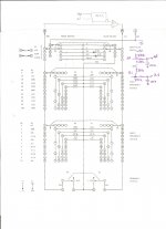
I’m attaching a revised version of my earlier sketch that should offer better consistency with Heath’s original assignment of circuit nodes--- specifically points H, J, and K. It also shows the tap points E0 and E1 that I’m suggesting.
For convenience I’m also re-posting one of Jack’s very useful drawings.
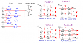
I really like Jack’s detailing of the capacitor range switching and “Key” linkage to four corresponding switch positions, A through D. The “virtual LEDs” conveniently indicate the state of the switch taps: a “lit” LED indicates the tap is at +15V = switch tap is open = logic 1. I’m attempting to retain that convention.
But I suspect a drafting error in the original drawing, since simultaneous closure of S3A and S4A (Key=A) would short the opamp output to ground and I wasn’t able to reconcile the LED states with capacitor switches.
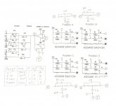
So with sincere apologies to Jack, I’ve taken the liberty of marking up his drawing with Wite-Out to show what I’m proposing. I’ve also added sketches of the Bridged-T networks associated with each range position; they show the associated position of tuning caps C1 through C4 and the E0 and E1 taps. An added table will help clarify, I hope.
Thanks for continuing scrutiny. This feels much like a preliminary design review--- a very useful exercise.
I’m attaching a revised version of my earlier sketch that should offer better consistency with Heath’s original assignment of circuit nodes--- specifically points H, J, and K. It also shows the tap points E0 and E1 that I’m suggesting.
For convenience I’m also re-posting one of Jack’s very useful drawings.
I really like Jack’s detailing of the capacitor range switching and “Key” linkage to four corresponding switch positions, A through D. The “virtual LEDs” conveniently indicate the state of the switch taps: a “lit” LED indicates the tap is at +15V = switch tap is open = logic 1. I’m attempting to retain that convention.
But I suspect a drafting error in the original drawing, since simultaneous closure of S3A and S4A (Key=A) would short the opamp output to ground and I wasn’t able to reconcile the LED states with capacitor switches.
So with sincere apologies to Jack, I’ve taken the liberty of marking up his drawing with Wite-Out to show what I’m proposing. I’ve also added sketches of the Bridged-T networks associated with each range position; they show the associated position of tuning caps C1 through C4 and the E0 and E1 taps. An added table will help clarify, I hope.
Thanks for continuing scrutiny. This feels much like a preliminary design review--- a very useful exercise.
Attachments
So with sincere apologies to Jack, I’ve taken the liberty of marking up his drawing with Wite-Out to show what I’m proposing.
Just an amusing side-bar. In the very early era of Wang Word Processors, I had a secretary, Debbie from Brooklyn, who had "Wite-Out" all over her CRT screen...I think they also called it "Sno-Pake".
My first job out of college in '71, our department had a Wang computer. I got to use it once or twice. I barely remember it. 😉
@pizzigri -- problem with your design is that it will be difficult to find SMT caps in both the form factor (0805, 1206, etc) and at a reasonable price.
so first get a BOM with parts you can actually purchase, that are reasonably sized. Search engines at Mouser and DK work well for this purpose.
Well.... I actually did it that way, searching each part at Mouser before modeling the board, I needed to know the footprint of each component. That is why there’s one Alu Pol cap - I wanted to avoid tantalum.
I saved the BOM...
Here’s the list, quantities and each price are missing - but its about 20 Euro, the mux alone is almost 5 Euro.
C1206F105K3RACAUTO
25V 1uF X7R 1206
C1206X106J3RACTU
25V 10uF X7R 1206 5%
VJ1206Y154JXXTW1BC
1206 0.15uF 25volts
12063C334K4Z2A
25V 0.33uF X7R 1206
C1206C155K3RACTU
25V 1.5uF X7R 1206
C1206C104K3GEC7210
25V 0.1uF C0G 1206
CRCW1206330KFKEA
1/4watt 330Kohms 1% 1206
VE-470M1ETR-0605
25 Volts 47uF 20% 6.
700-DG409DYT
DG409DY+T
I’m sorry for delay in responding.
I’m attaching a revised version of my earlier sketch that should offer better consistency with Heath’s original assignment of circuit nodes--- specifically points H, J, and K. It also shows the tap points E0 and E1 that I’m suggesting.
For convenience I’m also re-posting one of Jack’s very useful drawings.
I really like Jack’s detailing of the capacitor range switching and “Key” linkage to four corresponding switch positions, A through D. The “virtual LEDs” conveniently indicate the state of the switch taps: a “lit” LED indicates the tap is at +15V = switch tap is open = logic 1. I’m attempting to retain that convention.
But I suspect a drafting error in the original drawing, since simultaneous closure of S3A and S4A (Key=A) would short the opamp output to ground and I wasn’t able to reconcile the LED states with capacitor switches.
So with sincere apologies to Jack, I’ve taken the liberty of marking up his drawing with Wite-Out to show what I’m proposing. I’ve also added sketches of the Bridged-T networks associated with each range position; they show the associated position of tuning caps C1 through C4 and the E0 and E1 taps. An added table will help clarify, I hope.
Thanks for continuing scrutiny. This feels much like a preliminary design review--- a very useful exercise.
Uhhh now I’m lost again, plus - we don’t need a level shift to pull EN low? Help....
My contention is that we don't need the conditioning network on the EN pin but, as a bit of reassurance, your layout should work as is--- it's sufficiently flexible to accommodate the eventual outcome.Uhhh now I’m lost again, plus - we don’t need a level shift to pull EN low? Help....
Anything I can do to reduce confusion?
I can suggest a simple experiment performed on a IG-18 for added confidence:
With a dual channel scope, simply clip DC-coupled scope probes to capacitor leads on the range switch to sense E0 and E1. As the range switch is exercised, each probe should present one of three waveforms: an open path should display near 0V due to 1Meg or 10Meg scope load; DC bias about 21VDC (J); or large sine wave (H).
Connect E0, E1 as Steve indicates, do not connect EN
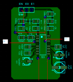
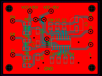
This is a layout I am working on. The olive green is the top layer with a copper pour attached to the "BLACK". "BLACK" and "GND" meet up at the power supply.
This is a layout I am working on. The olive green is the top layer with a copper pour attached to the "BLACK". "BLACK" and "GND" meet up at the power supply.
Attachments
Last edited:
My contention is that we don't need the conditioning network on the EN pin but, as a bit of reassurance, your layout should work as is--- it's sufficiently flexible to accommodate the eventual outcome.
Anything I can do to reduce confusion?
I can suggest a simple experiment performed on a IG-18 for added confidence:
With a dual channel scope, simply clip DC-coupled scope probes to capacitor leads on the range switch to sense E0 and E1. As the range switch is exercised, each probe should present one of three waveforms: an open path should display near 0V due to 1Meg or 10Meg scope load; DC bias about 21VDC (J); or large sine wave (H).
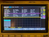
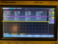
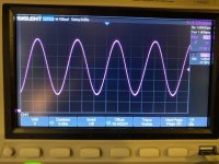
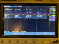
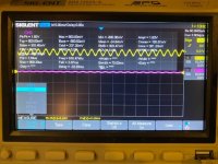
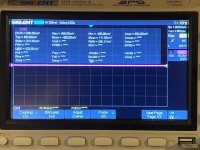
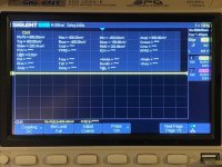
I had to come back home to do this... I connected both probes to the points you indicate: channel 1 to E0 on the rear wafer of the switch, on the .05uF lead; ch2 on the E1 point, rear lead of .005uF cap.
DC coupling, AUTO trigger, 2v divisions, each probe set at 10x.
Well, what I end up with is the following.
1x, E0 and E1 flat line.
10x, E0 sine wave, 50Hz, pk-pk 16V, E1 flat line;
100x, E0 sine wave, 50Hz, pk-pk 16V, E1, sine wave, 50Hz, pk-pk 18V;
1000x, E0 flat line, E1 sine wave, 50Hz, pk-pk 18V.
Maybe I'm doing something wrong? GND is to chassis, at the nearest point to the test points.
Last edited:
Very informative! I see that you have added the two resistors and cap to the EN sense line. And that you use electrolithics also for the 10 and 1.5 uF caps.Connect E0, E1 as Steve indicates, do not connect EN
This is a layout I am working on. The olive green is the top layer with a copper pour attached to the "BLACK". "BLACK" and "GND" meet up at the power supply.
I was uder the impression that MLCC C0G (NP0) where to be preferred, so that is why I drafted the board that way. And the 47uF is a polymer Al.... the quality here is not so important?
Also, I wanted to do the same for the ground, but I could not figure out how to turn a copper fill into a gnd layer in freaking diptrace, and allow the program to "see" it as a GND "net" so that it would maintain all component relationships.
I had to come back home to do this... I connected both probes to the points you indicate: channel 1 to E0 on the rear wafer of the switch, on the .05uF lead; ch2 on the E1 point, rear lead of .005uF cap.
DC coupling, AUTO trigger, 2v divisions, each probe set at 10x.
Well, what I end up with is the following.
1x, E0 and E1 flat line.
10x, E0 sine wave, 50Hz, pk-pk 16V, E1 flat line;
100x, E0 sine wave, 50Hz, pk-pk 16V, E1, sine wave, 50Hz, pk-pk 18V;
1000x, E0 flat line, E1 sine wave, 50Hz, pk-pk 18V.
Maybe I'm doing something wrong? GND is to chassis, at the nearest point to the test points.
You've mentioned the correct range capacitors but I believe the points of interest are on the front deck, nearest the the front panel.
I should have mentioned that the IG-18 has circuit common floating with respect to the chassis. That may be why you're seeing significant hum. Try joining them together (e.g. via green and black biding posts) and repeating the experiment.
Please let me know if this doesn't produce good results.
Steve

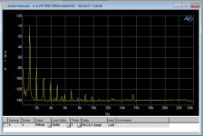
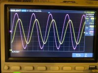
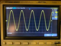
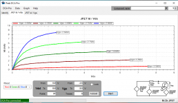
So here are the images. Took some time to figure how to show the info.
They are in sequence: 1x, then 10x 100x and 1000x last.
I also measured them; A is the measure of channel 1 (that is connecte to E0), B is the measure of channel 2 (E1), and C is the sine waveform that I get on 10x, 100x and 1000x with the frequency read by the scope. Sorry, I wish i was more competent in EE.
Attachments
-
 1000xb.jpg99.5 KB · Views: 96
 -
 1000xa.jpg96.1 KB · Views: 107
 -
 100xc.jpg74.6 KB · Views: 108
 -
 100xb.jpg99.8 KB · Views: 109
 -
 100xa.jpg98.7 KB · Views: 116
 -
 10xc.jpg85 KB · Views: 102
 -
 10xb.jpg86.4 KB · Views: 170
 -
 10xa.jpg88.6 KB · Views: 176
 -
 1xb.jpg85.3 KB · Views: 174
 -
 1xa.jpg83.4 KB · Views: 184
Thank you, Franco. I believe your measurements add confidence that the technique should work as envisaged.
I think your images 1,3,6, and 9 tell the story (1xa, 10xa, 100xa, 1000xa); if you watch the scope as you rotate the range switch through its four positions, you'll see four different "state" traces presented.
To contrast the IG-18/339 versus the IG-18, note that the /339 circuit has the oscillator opamp biased at ground, but the IG-18 biases at about 20VDC. This elevated bias makes the scope measurement very simple. An open capacitor path is revealed when the scope DC load pulls the trace to ground. (The IG-18/339 pull-up trick pulls open paths to +15V.) IG-18 active capacitor paths are biased to about 20V; IG-18/339 have bias at ground.
So if you construct a truth table in which an open cap path is coded as 1, and a biased path is coded as 0, you will get the same table in both cases. (post #122)
What is your source for the two orange 2% caps? They are polypropylene?
Thanks.
Steve
OK, so I should stick to table in post 122 I imagine.
The caps you see in the pic are the original range caps I found in the IG18 I got from Ebay. I tried finding 2% or even 1% caps and they're either darn impossible to find in the right value or crazy expensive. I mean tens of dollars each expensive.
I am still triyng to understand why you deem the conditioning network on the EN pin unnecessary, but Jack instead does.
I also tried comparing the layout of my board to Jack's and I see something I can't understand.
Jack, in your schematic (and in the original Lafferty schematic) we have four connections from the switch: N-violet, O-orange, P-blue and L-green, L being also "dirty" GND. See post #87 and #114.
In your board layout for SMD fabrication, post #128, I instead only see three outputs: P and O, which come out of the mux (pins 8 and 9 respectively), and L (which is the ground plane of the board).
Incidentally, the polarity of C25 is then inverted compared to your schematic... and connected to GND. I thought that the rail coming out of pins 10,11,12 was to be connected to N, which is apparently not wired but merged with GND.
So, to recap, what it seems to me is that switch side S1B is wired as it should according to all schematics, while side S1E is inverted and its output omitted.
What am I missing?
Hi Franco,
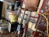
It hadn't occurred to me that Heath might have had varying capacitor procurement. Below is a pic of the IG-18 I bought from a friend. Two caps are Electrocube brand and at least one is branded "Standard."
Would you describe your project objective? What would you like to implement as a first step? Are you still intending to develop a satellite board that is an add-on to a Lafferty/Moore design? Remember, your existing layout is flexible, so you can proceed with little risk. The conditioning network can be populated without connecting the enable line to the range switch; the network will assert the Enable pin continuously.
Regards,
Steve
Attachments
Steve,
i am basically moving forward in steps. I was following EEVBlog's infinite thread on super pure oscillator design and came to know about the IG18 and the sort of cult following it has. So I got one for not so cheap on ebay (due to shipping and taxes to EU) and tried to improve it. First by the obvious and various little mods, then moving to alternative designs. Among them, the Moore/Lafferty, which I like best. I learned to draft in DipTrace (very badly) as this ECAD is highly regarded in EEVBlog as being easy to use, affordable and with many features ...
Be as it may, I completely redrafted Burke's board of Lafferty's design (with Stephen's help and support BTW!!).
I also replaced the old PS circuit with a 317/337 design, and had to purchase a 18+18V trafo as the original has an excessively high voltage output (the board I made can be easily used wiring your trafo for 240 and using it with 110V in the USA).
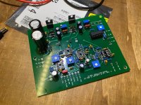
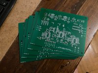
I already fabbed five boards - BTW, if you want one, just ask - and I actually stuffed one, you can see it in one of the pics.
But I found out that rotary switches have become expensive, not readily available and difficult to use. Plus, most of the parts used in Lafferty's design are either unobtainable, or expensive as gold (I mean, 15 years ago you could get a 2N4092 for pennies,now they're like 6 $ each!!!!).
As I already said, a complete 1% caps set for the range is outrageously expensive, alternative is lose a lot of time and space padding groups of caps to reach the values, but why not just use what's there?
So Dick's idea to use the original range caps. Still, either finding additional decks to mod the switch or a new switch for the AGC caps did not appeal to me.
The original Heath notch filter switches already use 1% resistors, but the attenuator uses 10% carbon parts; I ordered 1% Vishay metal film resistors (all of them in 10-20 for each value costed less than 10$) and will rewire the attenuator switch as Moore suggested, using the HP239A design.
The future goal is actually to redesign completely the circuit in SMD. The world moved on since Lafferty and Moore published their work, better spec parts are available as SMD, replacing the FET with a possibly better SMD part, all of the circuit smaller, with good GND planes (and maybe even additional shielding) and taking less real estate on the board.
Integrating the mux and agc caps into the board, and maybe even a better output amp (jackinnj design that he showcased here gave me the idea) and move out of the board the PS to place it where the original was.
For now though...
To try out the design, I wanted to just replace the rotary switch and build the additional daughterboard with the mux, if both you guys validate my PCB!
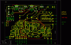
Here are some pics of my progress. The mux board now features connected GND planes ! I figured out that feature, it was right in front of my face all this time. Argh.
i am basically moving forward in steps. I was following EEVBlog's infinite thread on super pure oscillator design and came to know about the IG18 and the sort of cult following it has. So I got one for not so cheap on ebay (due to shipping and taxes to EU) and tried to improve it. First by the obvious and various little mods, then moving to alternative designs. Among them, the Moore/Lafferty, which I like best. I learned to draft in DipTrace (very badly) as this ECAD is highly regarded in EEVBlog as being easy to use, affordable and with many features ...
Be as it may, I completely redrafted Burke's board of Lafferty's design (with Stephen's help and support BTW!!).
I also replaced the old PS circuit with a 317/337 design, and had to purchase a 18+18V trafo as the original has an excessively high voltage output (the board I made can be easily used wiring your trafo for 240 and using it with 110V in the USA).
I already fabbed five boards - BTW, if you want one, just ask - and I actually stuffed one, you can see it in one of the pics.
But I found out that rotary switches have become expensive, not readily available and difficult to use. Plus, most of the parts used in Lafferty's design are either unobtainable, or expensive as gold (I mean, 15 years ago you could get a 2N4092 for pennies,now they're like 6 $ each!!!!).
As I already said, a complete 1% caps set for the range is outrageously expensive, alternative is lose a lot of time and space padding groups of caps to reach the values, but why not just use what's there?
So Dick's idea to use the original range caps. Still, either finding additional decks to mod the switch or a new switch for the AGC caps did not appeal to me.
The original Heath notch filter switches already use 1% resistors, but the attenuator uses 10% carbon parts; I ordered 1% Vishay metal film resistors (all of them in 10-20 for each value costed less than 10$) and will rewire the attenuator switch as Moore suggested, using the HP239A design.
The future goal is actually to redesign completely the circuit in SMD. The world moved on since Lafferty and Moore published their work, better spec parts are available as SMD, replacing the FET with a possibly better SMD part, all of the circuit smaller, with good GND planes (and maybe even additional shielding) and taking less real estate on the board.
Integrating the mux and agc caps into the board, and maybe even a better output amp (jackinnj design that he showcased here gave me the idea) and move out of the board the PS to place it where the original was.
For now though...
To try out the design, I wanted to just replace the rotary switch and build the additional daughterboard with the mux, if both you guys validate my PCB!
Here are some pics of my progress. The mux board now features connected GND planes ! I figured out that feature, it was right in front of my face all this time. Argh.
Attachments
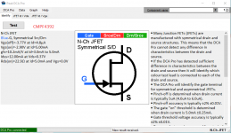
CMPF4392 is getting close to 2N4092. 2N4092 has noise referenced at 1.2nV/Rt Hz whereas CMPF4392 is not specified. (MMBF4392 is also close but now obsolete)
Attachments

Last edited:
- Home
- Design & Build
- Equipment & Tools
- Heath IG-18 IG-5218