After sleeping on it, I have a come up with a battle plan:
I can run with the 12 VAC transformer I got by mistake, keeping almost all the components as they are. All I need to do is replace the zeners with 12V types, which I already have on hand. It runs at higher currents than I planned, but as I discovered yesterday the transistors can support more heat than I thought, and R12,13 at 1R cut the output current (and heat) more than I calculated, so the end result is pretty close to what I originally planned for in terms of output power and bias current.
So step one is to replace the zeners.
Step two is to stop with the op amp stage oscillating. As I wrote above this should not be too difficult, it's already touch-and-go stable.
Step three is to test this version for noise, ringing, and frequency response, and try changing R12,13 to evaluate thermal stability.
Step four is to case up this version, check for ground loops and noise pickup in the chassis, and give it a listen.
Then I will present the slightly revised, final schematic and board layout. The standard version will be rescaled from my prototype to match 9VAC secondaries, though an alternative 12VAC version will be included as many people will be re-using supplies from Phonoclone / VSPS projects.
Today's update.
Up and running with 12V Zeners, driver current doubles but output transistor current is half of what it was before, only 6 mA. Driver transistors a bit too warm.
Op amp stage is stable with 100 ohm across the input, picks up noise when open circuit, as before.
From the output current ratios, estimate that R12,13 should be set at 12/(driver current in mA). Will change from 1 ohm to 0.5 ohm tomorrow, as well as switch R10,11 to something larger to cool everything down.
First Results
V++ 15 V
V+ 11 V
R10,11 360R
R12,13 1R
R14 47R
Q3,4 at 28 mA, Q5,6 at 9 mA.
Diamond buffer open loop.
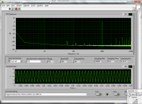
So here's the prototype on the bench, pumping out 1 V rms into a 15 Ohm resistive load, with the buffer outside the feedback loop. That's 100 mA peak output current, hard into class B.
0 rms noise baseline shown for reference, note the output DC offset voltage is only 2 mV.
~0.0001% distortion at 66 mW into 15 ohms open loop. Holy craptasticles Batman!
V++ 15 V
V+ 11 V
R10,11 360R
R12,13 1R
R14 47R
Q3,4 at 28 mA, Q5,6 at 9 mA.
Diamond buffer open loop.
So here's the prototype on the bench, pumping out 1 V rms into a 15 Ohm resistive load, with the buffer outside the feedback loop. That's 100 mA peak output current, hard into class B.
0 rms noise baseline shown for reference, note the output DC offset voltage is only 2 mV.
~0.0001% distortion at 66 mW into 15 ohms open loop. Holy craptasticles Batman!
Attachments
Last edited:
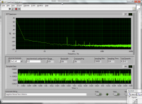
PS The harmonics of the 1 kHz sine are mostly artifacts from the (digitally generated) sine wave signal rather than distortion from the amplifier itself. Anything below -80 dB for the sine harmonics is likely generated by the source. The power supply hum at 60 Hz is most likely stray pickup as the power transformer and circuit board were just sitting open on my desk.
Attached is the 100 Hz sinewave, measured as above, where distortion caused by the digital artifacts on the input signal are more clearly seen. The point is the amplifier distortion is at least at this level or less. The only distortion measurable is the third harmonic at -80 dB. For smaller signals within class A operation basically you are just left with the spurious peaks at -90 dB and below. I cannot measure distortion levels below -80 dB without getting a better function generator.
Attached is the 100 Hz sinewave, measured as above, where distortion caused by the digital artifacts on the input signal are more clearly seen. The point is the amplifier distortion is at least at this level or less. The only distortion measurable is the third harmonic at -80 dB. For smaller signals within class A operation basically you are just left with the spurious peaks at -90 dB and below. I cannot measure distortion levels below -80 dB without getting a better function generator.
Attachments
Last edited:

How do you compute that ~0.0001% thd figure, when you have about 0.012% of H5 ?
edit: btw, such a figure is already pretty good. It beats the 4 transistors, 6 resistors simple diamond buffer by far and should be quite close to a full blown one (with ccs and the like).
Last edited:
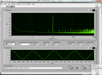
A couple more, last for today. The -20 dB sine wave is clean but for the artifacts from the function generator and a little bit of hum. The 10 khz 1 V square pulse is looks good.
00940: 0.0001 or .01%, sorry I neglected to multiply by 100 when typing the % sign in there.
Thanks for keeping me honest. I appreciate it.
/R
00940: 0.0001 or .01%, sorry I neglected to multiply by 100 when typing the % sign in there.
Thanks for keeping me honest. I appreciate it.
/R
Attachments


Why not make current stage in Class A?
Bias 50 mA for example will not make much heat (=small heatsinks)
and does not load the transformer much.
Try. You will get lower distortion.
Class A is the Rolls Royce of amplifiers.
Bias 50 mA for example will not make much heat (=small heatsinks)
and does not load the transformer much.
Try. You will get lower distortion.
Class A is the Rolls Royce of amplifiers.
> Q3,4 at 28 mA, Q5,6 at 9 mA.
> Diamond buffer open loop.
Should be the other way. Q3,4 is way too much current.
Q3,4 at 5 mA
Q5,6 at 50 mA
What transistors do you use?
> Diamond buffer open loop.
Should be the other way. Q3,4 is way too much current.
Q3,4 at 5 mA
Q5,6 at 50 mA
What transistors do you use?
Put a lowpass filter on the input. You could solder 330-470pF across R6. This should stop the opamp picking up RF crap which could be causing oscillation.
@jaycee: Funnily enough I didn't see any oscillation yesterday when everything was hooked up. You are right I think: R6 likely to be the source of the noise pickup, so putting the cap on R6 should effectively solve any residual problem. (When an input signal is connected, R6 is in parallel with the input impedance, effectively shorting out the noise anyway, but it will may get noisy without an input attached.
@lineup: I do understand your points, really. Yes it probably does seem backwards to you, but there is a method to my madness. Transistors are BD135/6, and the drivers run hotter than the outputs by design, as insurance, to stop thermal runaway on the output stage. Later I will have the transistors in thermal feedback, and this will keep the currents more closely balanced.
@lineup: I do understand your points, really. Yes it probably does seem backwards to you, but there is a method to my madness. Transistors are BD135/6, and the drivers run hotter than the outputs by design, as insurance, to stop thermal runaway on the output stage. Later I will have the transistors in thermal feedback, and this will keep the currents more closely balanced.
00940: 0.0001 or .01%, sorry I neglected to multiply by 100 when typing the % sign in there.
It makes sense. 🙂
Now, what would be interesting are distortion measurements with the buffer inside the loop. 😉
Also... 47r at the output is quite a lot. With a 15r load, you're wasting a lot of power accross it. You probably could reduce it to 4.7r or even get rid of it. See : http://www.diyaudio.com/forums/head...allowable-headphone-amp-output-impedance.html
Unfortunately it's unlikely to be measurable with my equipment. I need a ultra-low distortion oscillator, instead I'm using a 250kHz, 16bit DAC.
About the series output resistance, remember the transistor idle power is far higher than the output power. Putting 10 mA though 15 ohms and putting it through 15+47 ohms doesn't change the circuit heat output much, and there is sufficient voltage headroom to do it without clipping.
About the series output resistance, remember the transistor idle power is far higher than the output power. Putting 10 mA though 15 ohms and putting it through 15+47 ohms doesn't change the circuit heat output much, and there is sufficient voltage headroom to do it without clipping.
It's not only a problem of wasted power. 47r is high enough to significantly alter the frequency response of some low impedance headphones.
As you know the series resistance is there to linearize the output power vs. headphone impedance for a given volume setting. It also provides some isolation between the output and the cable capacitance, which can be a an issue for high feedback circuits, unlikely to be an issue if the buffer is open loop.
It's optional: it the headphone impedance isn't resistive over the audio spectrum then it can be removed or significantly reduced.
Now I'm going to read that link you posted in full. It looked interesting.
It's optional: it the headphone impedance isn't resistive over the audio spectrum then it can be removed or significantly reduced.
Now I'm going to read that link you posted in full. It looked interesting.
I basically agree with the points in that thread.
- the 120 ohm standard was an attempt to normalize the volume settings for different headphone impedances, and cannot be interpreted to mean that headphones are optimized for use with this series resistance.
- headphone impedance is much flatter than speaker impedances, such that <100 ohm series resistance does not cause excessive deviation in frequency response except in extreme cases.
- the anecdotal evidence is consistent and suggests zero or near zero values sound best
I have both 300 and 16 ohm headphones, and for convenience of being able to use both at normal volume settings I'm going to include 47 ohms in series. I will update the web page to make it clear that it is optional, and can be replaced by a much smaller value, with a reduction in R7 from 10k to 4k7 to compensate.
So here's a preview showing where I'm headed with the next board layout.
1. Small heatsinks, and driver and output transistors share a heatsink to stay thermally coupled. This is what I meant earlier by "thermal feedback" and it keeps the output transistors running at bias currents close to those of the driver transistors.
2. Tidied up the A-B1-B2 feedback jumper pads. R14 is now inside the buffer feedback connection, for trace layout reasons. When using the A-B2 connection, R14 should be reduced to zero or 1-2 ohms.
3. C0 is included as an optional bypass of C6.
Attachments

Significant reworking of the Sapphire home page.
Took 00940's and lineup's suggestions to heart, R14 is now 1 ohm, and the gain is 15 dB. One version, one parts list. Keeping it simple.
Took 00940's and lineup's suggestions to heart, R14 is now 1 ohm, and the gain is 15 dB. One version, one parts list. Keeping it simple.
I have changed my mind.
If you can get open-loop THD 0.010% it is good.
It requires a lot to get lower.
Like 10mA + 100mA bias of stages.
So, if you can some way get like 0.010% it is very good.
If you can get open-loop THD 0.010% it is good.
It requires a lot to get lower.
Like 10mA + 100mA bias of stages.
So, if you can some way get like 0.010% it is very good.
The amp gives 0.01% under 60 mW into 15 ohms, for any "normal" situation it is less, and if the output stage can be kept in class-A, less again.
My goal is to use the thermal coupling to bring the output stage bias up to 20-25 mA, for about 10 mW class-A into 16 ohms.
(16 ohm phones are the "worst case" for current needs, high impedance phones get much more power for the same current.)
My goal is to use the thermal coupling to bring the output stage bias up to 20-25 mA, for about 10 mW class-A into 16 ohms.
(16 ohm phones are the "worst case" for current needs, high impedance phones get much more power for the same current.)
Last edited:
- Status
- Not open for further replies.
- Home
- Amplifiers
- Solid State
- Headphone amplifier drop-in replacement for Phonoclone 3 and VSPS300