Greetings,
Today I have successfully tested a new I/V stage I designed to be used with the PCM1794A and the ESS9008 (though it will work with almost any current output DAC).
The design is loosely based on Nelson Pass' D1 MOSFET I/V stage, but my circuit has some unique features.
I chose to use a CCS load for both the casocde and the output emitter follower. I also made use of parallel devices (because the DACs I am using put out a lot of current) and voltage references. Obviously I chose BJTs instead of FETs and I also use +15V and -5V.
I have not measured it yet, but it sounds great. The simulations look very good, but I know they can't really be relied on.
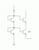
Here is the CCT schematic. I hope some of you find some use for it in your own projects.
The circuit as shown is configured for the Buffalo(ESS9008) DAC with balanced output of 2VRMs at 0db.
VR3/VR4 set the bias current through the common base amplifier. I found the best results so far by adjusting these until the voltage at the bases of Q11/Q12 was about 6V
VR1/VR2 are used to adjust the voltage at the virtual GND input to 0V
As always, any constructive feedback welcome.
Cheers!
Russ
Today I have successfully tested a new I/V stage I designed to be used with the PCM1794A and the ESS9008 (though it will work with almost any current output DAC).
The design is loosely based on Nelson Pass' D1 MOSFET I/V stage, but my circuit has some unique features.
I chose to use a CCS load for both the casocde and the output emitter follower. I also made use of parallel devices (because the DACs I am using put out a lot of current) and voltage references. Obviously I chose BJTs instead of FETs and I also use +15V and -5V.
I have not measured it yet, but it sounds great. The simulations look very good, but I know they can't really be relied on.
Here is the CCT schematic. I hope some of you find some use for it in your own projects.
The circuit as shown is configured for the Buffalo(ESS9008) DAC with balanced output of 2VRMs at 0db.
VR3/VR4 set the bias current through the common base amplifier. I found the best results so far by adjusting these until the voltage at the bases of Q11/Q12 was about 6V
VR1/VR2 are used to adjust the voltage at the virtual GND input to 0V
As always, any constructive feedback welcome.
Cheers!
Russ
Attachments
Looks very interesting to me, Russ, as I'm a fan of Nelson Pass' work. I'll be keeping my eye towards this thread and possible IVY vs. Haiku comparisons.
THX Russ, great ! What need to be changed to make it work as well with a 1794 ? Can you give us the correct values for that one, too ? THX a lot !
THX Russ, great ! What need to be changed to make it work as well with a 1794 ? Can you give us the correct values for that one, too ? THX a lot !
And TDA1541 too 😀
Interesting circuit. I have considered a setup like this myself. Although I never came to a physical implementation of my ideas, and your I/V concept looks really mature to me, I would like to share some contemplations I had when drawing mine up.
I wonder (nitpicking alert!), wouldn't your current sources be more stable hen you connect the ref input of the TL431 to the emitter of one of the current source transistors, instead of to its base? See page 6 on the Fairchild datasheet .
Furthermore, I would consider to generate the base voltage for Q5/6 with an identical transistor connected as a diode with the same bias current, to add thermal tracking. If that's not enough still, it might even be an idea to cascode Q5 and Q6 with an additional transistor, biased by another diode connected transistor in series with the base bias transistor, so both Q5/6 and their base bias transistors have identical Vce, identical dissipation and, when mounted in thermal contact, very good thermal tracking. This ensures that your DAC current output stays at 0V over a wide temperature range.
I didn't find an off-zero output voltage tolerance specification in many DAC datasheets (the TDA1541A sheet states 25 mV though as an exception), but many state that the current output should be held to GND as close as possible.
On the workbench, the benefits of these measures might not stand out immediately or even at all. But in an enclosure, with no knowledge where it is going to be used (on a cold floor, close to a warm lamp, or on top of a hot amplifier), thermal tracking might even prevent a situation where, on one occasion, sound is stellar, and on the other it sounds only so-so. The latter usually occurs when friends are around...
Another thought that popped into my mind during lunch break: isn't it a good idea to use a folded cascode? That way, all signals are referred to ground. In the current situation, the output signal is referred to the positive supply, resulting in practically nonexistent PSRR. The demands on the power supply are quite severe this way.
Wow Timpert, a lot to cover. 🙂 Thanks for the comments and the input.
I may try changing the VREFs as you suggest, but in practice the way I have them seems to be working great.
The base voltage for Q5/Q6 needs to be adjustable to zero the virtual ground. I am not sure how I would accomplish that using your scheme.
In practice the circuit seems to be thermally stable. I have heated it with a heat gun and the input node only moved about 5mv. 🙂
The current through the rest of the circuit is less critical.
I thought about a folded cascode too, and I may try it, but it makes the cct more complex than it really has to be. With a good power supply like the LCBPS things should be just fine. It certianly has no worse PSRR than a D1. 🙂
Cheers!
Russ
Blitz said:THX Russ, great ! What need to be changed to make it work as well with a 1794 ? Can you give us the correct values for that one, too ? THX a lot !
1.07K for R1A-C R2A-C (1K would be fine too)
Then you simply need to adjust the pots as described earlier.
Cheers!
Russ
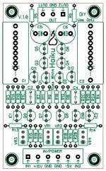
I'm always impressed with the things you manage to fit on those tiny PCBs, Russ, and a discrete balanced I/V is a real triumph.
I'll get one anyway, because you make these things fun and easy, but for a future upgrade, you want to think about replacing the board space occupied by those two huge capacitors with a well-designed servo?
I'll get one anyway, because you make these things fun and easy, but for a future upgrade, you want to think about replacing the board space occupied by those two huge capacitors with a well-designed servo?
Hence the nitpicking alert 😉I may try changing the VREFs as you suggest, but in practice the way I have them seems to be working great.
The idea behind my scheme is to generate the base voltage required to get an emitter voltage at Q5/6 of 0V by subjecting an identical transistor, connected as diode, to an identical current, and using the resulting base voltage as bias for Q5/6. To ensure that Vce is also identical (or very close) to that of the bias transistor, the second diode connected transistor plus the cascode transistor are included. In this way, both current and voltage for the bias transistor and for Q5/Q6 are identical, meaning identical dissipation, and identical temperature rise.
You could even consider eliminating one bias source and connecting both bases of Q5 and Q6 together to the same bias voltage. This way, the AC base currents cancel out due to differential operation.
If your transistors are identical (not of the same type, but really identical) the above will work and you'll get 0 V on the emitter of Q5/6 if biased like in my figure. And you get 100% thermal tracking because the bias and amplifier transistors are equally warm on the outside and dissipate the same. Even the most picky DAC will always perform as intended this way.
In practice, you'll only achieve this when both transistors are on the same silicon die, or very well matched by their Vbe/Ic characteristics. If you manage this with two transistors, then you'd naturally use them in in the position of Q5 and 6 and use the leftovers for the bias. Therefore, if you make the current source in my figure adjustable, then you can slightly change the voltage across the bias transistors by changing the current through them.
This all sounds like nitpicking XXL, but isn't this what the hobby is all about? 😉 Otherwise, I don't intend to say you should do all this, but I hope I've given you some inspiration for further refinement, since there is clearly still room left for experimentation.
Timpert, I am always happy to hear from folks like you I appreciate the food for thought.
Yes I think I see what your getting at with your VB scheme for Q5/Q6. In practice I think it may be difficult to get right.
As I have not seen any serious thermal drift I am happy for now. I can live with 5mv or so.
One other note here. One of the design goals was to make it all fit on a rather smallish PCB 2" x 3.3". This is one reason why the two current sources share a common VREF this is the reason the ref node is not connected to an emitter.
I am struggling a bit with the folded cascode implementation, so if you have an idea there I would be glad to see it, especially if it could be done with just a couple more Qs.
Thank you very much for your interest.
Cheers!
Russ
Trivial point about PSRR.
Although the single sided PSRR is small, the PSRR in balanced operation is more or less the CMRR of the following stage, which should be more than good enough, given the high signal levels. This assumes R1A-C and R2A-C are well matched.
For example, even if the +15V supply is pretty nasty (say a 7815 with 10mV of broadband yuckiness), as little as 60dB of CMRR in the next stage pulls this down to 10uV, which is 106dB down on 2V.
PigletsDad said:Trivial point about PSRR.
Actually this is a very good point. 🙂
Very glad to see your interest.
Cheers!
Russ
Not true. The whole point of going for differential is to be more immune to noise and interference coming from the outside, and to double the available signal swing within the range of the power supply (and therefore improving SNR by 3dB, all other things being equal). It is definitely not intended to provide the designer more margin for compromises on signal integrity. At least, that's my personal attitude in this issue. Why double the amount of semiconductors, and after that allow yourself to squander the benefits it gives you? Furthermore, if someone wants to connect an amp that only accepts single ended signals (which most amps do), with a totally clean source he/she's free to do so. But not with a source that is only clean in the differential sense.Trivial point about PSRR.
Russ, I think that most difficulty lies in the required match of the transistors. If you want to sell your stuff in kit form, that might not be practicable, agreed. I can only imagine the ways that customers invent to mix up matched transistors that all look exactly the same on the outside. If it were for personal use, I'd go for it, but in kits to sell, I would shy away from it too. I didn't take that aspect into account.
A folded cascode will take several more transistors per leg (so it will easily run into 10 or more total) if all the additional current sources are counted as well. Most difficult part will be a current source from the positive rail that is coupled to the one from the negative rail, so the current outputs will track. Although the cascode itself is only one extra transistor, it's the biasing that kills off the idea when space is tight. I could draw up something, but that will have to wait until tomorrow.
Timepert,
I am still investigating your ideas.
I can see your point on PSRR especially as it relates to single ended signals, but this I/V is not really intended for single ended output.
I have no problem using an opamp for the summing. Then you should still get a good clean signal from the whole rig.
On my case I would just use the last half of my own IVY board.
Cheers!
Russ
What about something like this...
I just tested it and even with pretty poorly matched Qs it seems to track pretty well. Less than 2mV drift when heated a good 30 degrees.
And it the nice thing is it does not effect the layout much. It just swaps one resistor for one transistor, and moves the pot.
I simulated it first like this:
I just tested it and even with pretty poorly matched Qs it seems to track pretty well. Less than 2mV drift when heated a good 30 degrees.
And it the nice thing is it does not effect the layout much. It just swaps one resistor for one transistor, and moves the pot.
I simulated it first like this:
Attachments
- Status
- Not open for further replies.
- Home
- Source & Line
- Digital Source
- Haiku I/V Stage