Hi Rick,
Yes I did read that, and addressed that point for you. Then because of the nature of your comments, I posted a complete response.
Hi phase,
-Chris
Yes I did read that, and addressed that point for you. Then because of the nature of your comments, I posted a complete response.
I did explain how my answer related to this amplifier design.lets get back to DH-200/220 mods please,
Well, that would be a big error. You need to match hFE, not VBE. To read hFE and compare the devices, the die have to be at the same temperature. Otherwise the numbers will not show you a value that you can relate to another device. Like I said, this is a real pain to do.I put in all Vbe matched devices
The grading is an overlapping range, so you can simply find and use the closest ones you can. It is a qualitative thing, not an absolute.KSA1381E and KSC3503D, they do not come in the same hfe grading anymore
Actually, your chances are somewhat better than winning a lottery.chances of find a match are like winning the lottery
I would counter by saying that no attempt to find close devices is a waste of money.= waste of time & $.
Hi phase,
Yes, exactly. You meant to say source resistors - yes?No emitter resistors in the original Hafler design either, so you can bet that there needs to be a matched set of outputs.
-Chris
Chris,
I will go with Mark Tillotson and Bob Cordell advise on audio amplifier design and build.
You can design and build your amplifiers the way you want, I will not challenge your design and build decisions anymore, but I will say that they have practical challenges for DIYAudio members, with no demonstrated benefit.
If forum members want to follow your points of view, it is fine with me, but I will not be following your impractical advise, end of this discussion for me. To each their own.
Did get a chuckle out this statement.
Say no more 🙄Actually, your chances are somewhat better than winning a lottery.
Last edited:
Hi Rick,
Do yourself a favor, read Douglas Self's books.
What I have suggested is impractical for high volume manufacturing, but in that situation they have turned to matched pairs in one case. The 2SA798 and 2SC1583 are good examples and have been found in audio equipment. The uPA68H is a dual JFet used in audio equipment too, in mass production. North American semiconductors have old numbers like the MAT series or some SSM devices. You can search for some 2N numbered devices often in the TO-78 case.
The average OP Amp depends on highly matched transistors to achieve the performance levels they do. Somehow I can't see Bob Cordell refuting the benefits of a matched differential pair.
Now, do you simulate circuits? If you do, there is an extremely effective exercise you can do that will prove this to you once and for all. Simply load a standard amplifier circuit, a blameless will do. Go to the diff pair and make one a different beta. So if you had a BC560 for example, go to the parts area and create BC560A and BC560B. In the characteristics table, simply make one beta something like 250 and the other one 350. This is a realistic possibility, so nothing so exaggerated so as to not apply to realistic situations you might actually see. Go back and specify one of the pair as BC560A and the other BC560B. Then run a simulation and look at the distortion and DC offset values. Run it again as it was using the diff pair both as BC560. You can do the same thing with BC550 if your diff pair is that polarity instead.
You don't need to report your findings, I know what to expect. So matching isn't important? Please explain the LM394 to us.
My advice is very practical for the DIYer. The entire point is to be able to build something better than what you normally would buy, and my advice is a practical way to achieve that. Buying say 20 small signal transistors is well within anyone's budget. It's just that more parts will deliver a higher yield of matched devices. Even if you only have 10, put the closest ones together. I do service and so buying 100 of them is practical for me.
You want a real answer on matching diff pairs? Ask Scott Wurcer. That man designed many chips and I think you can take his word over anyone else's on this subject. Walter Jung is another expert on this subject. Even John Curl, a working designer of audio circuits has an opinion that carries some weight. To be honest, I can't conceive of any professional design engineer of good audio equipment who would disagree with the concept of matching. An unbiased information source? An engineer that designs test equipment. The concept of a matched differential pair is central to the design of most linear amplifier types in the baseband range of frequencies. Things are rather different in RF, but modulator and demodulater chips also use a matched diff pair as a core requirement. Here's a CA3054 datasheet for your consideration. This is a dual diff pair with current source type tail current setup. You could look at a CA3089 schematic in this datasheet to see how diff pairs are used, and of course any standard op amp schematic. Most parts that any of us use will depend on matched differential pairs for high performance.
-Chris
You did not understand me saying that I am done with you last time!! So I will say it again,
I AM DONE WITH YOU!!
I AM DONE WITH YOU!!
🙂
I still have every right to respond to your comments. Especially when you accuse me of feeding people false information.
I have PM'd Bob Cordell to find out what his view is on matched differential pairs since you used him to refute what I was saying. Should be interesting. I'll be extremely interested to see what Bob's design of replacement circuit looks like. If it uses discrete transistors. maybe I will test it with and without matched pairs. But the next Hafler DH-220 / DH-200 I see, I will, especially for you, measure performance with and without matched pairs. Cool?
All,
This Hafler design pretty much depends on matched diff pairs in order to maintain low distortion and low DC offset. Other designs may use an offset trim control, but you shouldn't need to do that.
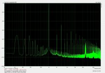
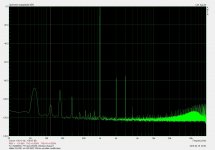
I have attached a before and after measurement on a Hafler DH-200 I repaired some time ago. The right channel measures about the same as the left channel. On this one I just moved the input transistors around to make better matches instead of using a tightly matched pair.
-Chris
I still have every right to respond to your comments. Especially when you accuse me of feeding people false information.
I have PM'd Bob Cordell to find out what his view is on matched differential pairs since you used him to refute what I was saying. Should be interesting. I'll be extremely interested to see what Bob's design of replacement circuit looks like. If it uses discrete transistors. maybe I will test it with and without matched pairs. But the next Hafler DH-220 / DH-200 I see, I will, especially for you, measure performance with and without matched pairs. Cool?
All,
This Hafler design pretty much depends on matched diff pairs in order to maintain low distortion and low DC offset. Other designs may use an offset trim control, but you shouldn't need to do that.
I have attached a before and after measurement on a Hafler DH-200 I repaired some time ago. The right channel measures about the same as the left channel. On this one I just moved the input transistors around to make better matches instead of using a tightly matched pair.
-Chris
Attachments
Hi Rick,
Well, Bob and I sharply disagree on this then with regard to matching input devices. I have proved this to be effective continuously over 30 + years. So it doesn't bother me at all that anyone might disagree with me as I have years of accumulated proof. I have measured significant drops in distortion simply by installing a close matched pair into an amplifier or gain stage.
......
Sorry for the long response, but there is good information in there. Your job, use it.
-Chris
Hi Chris,
I should have said more about transistor matching in my book – my bad. This conversation has reminded me of that.
This conversation has actually touched on at least four aspects of transistor matching. Vbe and beta matching in BJT input stages, and Vbe and beta matching in BJT output stages. It has also touched on matching issues for JFET input stages and MOSFET output stages. These are all different issues, and most are quite dependent on the particular circuit design. It is also important to bear in mind that when we say BJT transistor matching, we be clear about distinguishing between Vbe and beta matching.
While it is always a good thing to have matched devices in all aspects (as we often do in simulation), it is not always practical or economical enough to make a big enough improvement in performance to justify it in light of other priorities and sources of distortion that may be much larger. For example, in my experience with my amplifiers, output stage distortion has always been the biggest contributor, and it has not been difficult for me to get the IPS-VAS distortion down to miniscule levels.
Take, for example, a BJT IPS LTP. Perhaps the most important issue in keeping LTP distortion low (apart from degeneration) is keeping the transconductance of the two transistors the same. Transconductance in BJTs is quite predictable as a function of current for BJTs of the same type that are not even well-matched. This is why the use of a current mirror load for the IPS is so important. A perfect current mirror forces the operating currents of the two transistors in the pair to be virtually identical in an amplifier with significant negative feedback at low frequencies. This, in turn, causes the transconductances in the two devices to be nearly identical, largely independent of beta and Vbe mismatches. This is why Vbe matching in the current mirror is actually more important than Vbe matching in the LTP.
In both the LTP and current mirror, the effects of transistor mismatch are greatly mitigated by emitter degeneration. I typically use 10:1 degeneration in both, and of course with 1% resistors. 10:1 degeneration usually puts about 230-260 mV across the degeneration resistors. Differences in gm between the two LTP transistors will have the greatest effect on second harmonic distortion.
Vbe mismatch in the LTP of a well-designed amplifier with a current mirror load for the IPS will largely just result in a bit of output offset voltage of little consequence. Beta mismatch in the LTP transistors will mainly result in some output offset due to different base currents flowing in the DC resistances seen by the two bases – this is why we usually try to keep those DC resistances the same on both sides (and the lower the better). Beta mismatch in the LTP can often be a bigger contributor to output DC offset than Vbe mismatch. In either case, output offset voltage that is a consequence of Vbe or beta mismatch in the IPS LTP is usually not a significant contributor to distortion unless it is quite large. I usually like to use a DC servo to manage output DC offset. Among other things, this gives us more design freedom in choosing the DC resistances seen by the two bases of the LTP. It gets rid of the electrolytic shunt capacitor and allows the DC resistance on the feedback side to be different (lower) than that on the input side. This allows the use of low impedance feedback networks without requiring that the input impedance of the amplifier be low.
The effects of beta mismatch on distortion in an LTP are also reduced when the AC impedances seen by the transistors on each side are relatively low. This also reduces HF distortion from nonlinear Ccb transistor capacitances. This also pushes out in frequency the parasitic pole that is formed by the feedback network resistance against the input capacitance if the IPS.
I do not bother to hand-match BJT IPS LTP transistors, and still get extremely low IPS-VAS distortions in my amplifiers. I just use transistors out of the same tube. I always check the IPS-VAS distortion by taking the NFB from the pre-driver emitter resistor center tap and measuring amplifier distortion absent the output stage to make sure.
BTW, the distortion effects of Vbe or beta mismatches in BJT input stages can be easily seen in simulation by just using different models for the two devices, either with differing beta or differing Vbe.
The bottom line is that matching in IPS LTP transistors is good, but often is not as critical to distortion performance as we would think – but this does depend on the specifics of the amplifier design, with less well-executed designs likely being more affected by mismatch than really good designs.
Importantly, bear in mind that this is not to say that matching of beta and Vbe is not important in precision operational amplifiers, especially for DC characteristics like input offset voltage and input offset current, which are critical specifications for operational amplifiers. Even though the topologies of many audio amplifiers are similar to those of op amps, the practical real-world issues are not quite the same. The mission is different. The input offset voltage and input offset current are not as important as those for a general purpose precision operational amplifier that must provide high performance in a great variety of unforeseen circuit applications.
With JFET input stages, I always use a dual monolithic JFET matched pair, like the LSK389 or LSK489. It is still important to have a well-balanced current mirror load to force the two JFETs to operate at the same current. We still want the transconductances of those two JFETs to be the same. Just as with BJTs, the operating current in a JFET matters most in determining the gm. In fact, two JFETs from the same process that have different threshold voltages will still tend to have very similar gm if operated at the same current. JFETs nicely eliminate the issue of DC output offset due to input base current in BJT designs.
In complementary BJT output stages, it is almost futile to match beta (and Vbe) between the PNP and NPN devices, especially given that, even if matched at a static DC operating point, they are likely to become mismatched as their operating points vary widely with signal. Fortunately, a triple EF output stage has so much current gain that it drives the significance of beta mismatch to a very small effect. Not sufficiently so with only an output double. There are some output stage designs that do depend on P-N beta matching for optimum performance, however, even as triples – the Bryston output stage is an example.
Reasonably decent Vbe matching among the same-sex output transistors in the neighborhood of the quiescent bias current (50-200 mA) is helpful in reducing the tendency to current hogging and optimizing the benefits of the Oliver criteria for reduced crossover distortion (at least in theory). In my experience, Vbe matching of output transistors from the same tube is surprisingly good. In practice, Vbe matching will not be as good anyway, since the heat sink on which they are mounted is not perfectly isothermal. Only 1 degree C difference will cause two transistors to differ by more than 2 mV. With regard to current hogging, the most important thing is to use emitter resistors that are not too small and base stopper resistors that are not too large. I usually use 0.22 ohm emitter resistors and 2.2 ohm base stopper resistors. Those who use emitter resistors as low as 0.1 ohm are begging for current hogging problems in many designs.
In MOSFET output stages matching is much more important. Once again, not necessarily between opposite-sex devices, but surely among paralleled same-sex devices. This is so for two reasons. First, the variability of threshold voltages among MOSFETs is quite high. Secondly, because the use of source degeneration resistors is not very effective in mitigating the effects of offset – they need to be too large to help much.
Cheers,
Bob
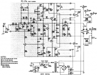
The spectra of the DH-200 posted above by Chris reminded me that there is an important design-dependent caveat to what I said in my overly-long post above. The Hafler design uses a fully complementary BJT input stage (NPN LTP + PNP LTP). In such a design input pair matching is important, since otherwise the two pairs may "want" different input offset voltages in the quiescent state. This means that they may fight each other for determination of the quiescent condition, often resulting in neither of them functioning at their best.
Further exacerbating the issue in the Hafler is that the IPS is not loaded with current mirrors, but just loaded single-endedly with a resistor. This adds another variable to achieving current balance between the pairs.
Finally, the input pairs do not seem to be strongly degenerated, so matching issues are not as strongly mitigated. By quick glance, it appears that LTP degeneration is only about 3:1.
So the bottom line here is that the Hafler and similar designs will be more sensitive to input pair matching, and their input pairs should be matched. However, the single-ended load resistors on the LTP should be carefully chosen to make the currents the same in the two transistors in each LTP, else the matching may be rendered for naught.
Cheers,
Bob
Hi Bob,
Thank you for explaining what I could not about device matching criteria.
In this thread below, I could not answer the question about adjusting the BALANCE pot P2 for lowest thd.
Repairing Hafler DH-120 Balance Adjustment
Can you explain how adjusting P2 minimizes thd?
Cheers
Rick
Thank you for explaining what I could not about device matching criteria.
In this thread below, I could not answer the question about adjusting the BALANCE pot P2 for lowest thd.
Repairing Hafler DH-120 Balance Adjustment
Can you explain how adjusting P2 minimizes thd?
Cheers
Rick
Attachments
Last edited:
The Hafler documentation makes no mention of any of these requirements.So the bottom line here is that the Hafler and similar designs will be more sensitive to input pair matching, and their input pairs should be matched. However, the single-ended load resistors on the LTP should be carefully chosen to make the currents the same in the two transistors in each LTP, else the matching may be rendered for naught.
Hi Rick,
They may not mention this, but looking at the circuit diagram tells you what you need to know. It is entirely possible that the person that designed the amplifier may not be aware of this for starters. I know of one person that used to work there, and specializes in this product line as rebuilds who hasn't got a clue.
You (not you, but everyone) need a broad range of experience in order to properly repair or modify equipment simply because these omissions are common in this industry. The repairer / modifier has to bring all the knowledge to the table when working on any product in case no mention is made of important factors. Just because someone designs a product and it is somewhat successful in the marketplace doesn't mean they are competent.
-Chris
From what I have read the DH-200 has been designed by Erno Borbely while he was working for Hafler. The DH-200 assembly kit however may not mention detailed design criteria information.
Here some history on Erno:
Author | Linear Audio
Fab
Here some history on Erno:
Author | Linear Audio
Fab
Last edited:
Hi Bob,
Thank you for explaining what I could not about device matching criteria.
In this thread below, I could not answer the question about adjusting the BALANCE pot P2 for lowest thd.
Repairing Hafler DH-120 Balance Adjustment
Can you explain how adjusting P2 minimizes thd?
Cheers
Rick
It looks like P2 adjusts the VAS bias current to an optimum value for low distortion. Not clear why this is without deeper analysis or even simulation. However, I would speculate there would be less need for the pot if a 2T VAS was used and if the IPS current mirror was degenerated. I have a Hafler SE-120 that I got on eBay, but have never tested it or looked inside.
Cheers,
Bob
Hi all,
I think P2 and P1 both can change the bias current of output's mosfets.
First, we may adjust the VAS current by P2. After this, output bias by P1.
So, the different pictures about distortion shown above may be just BIAS .
Question for designers in here...when replacing transistor sets, capacitors or even redesigning driver boards, how do you assure the feedback/control loop of the amp retains good gain and phase margin for stability.
Is there a bode plot analysis or something like that?
Is there a bode plot analysis or something like that?
Hi all,
I think P2 and P1 both can change the bias current of output's mosfets.
First, we may adjust the VAS current by P2. After this, output bias by P1.
So, the different pictures about distortion shown above may be just BIAS .
I believe you are correct about the effects of P1 and P2. P1 directly affects the output stage bias current in the usual way with the Vbe multiplier. P2 indirectly affects output stage bias by varying the VAS bias current, which has a minor effect on the voltage drop established by the Vbe multiplier bias spreader.
Cheers and Happy New Year,
Bob
Question for designers in here...when replacing transistor sets, capacitors or even redesigning driver boards, how do you assure the feedback/control loop of the amp retains good gain and phase margin for stability.
Is there a bode plot analysis or something like that?
This is a good question. The short answer is that if you are just replacing components with identical values, the original stability will be largely unaffected. If redesigning the complete circuit, or tweaking key component values, it is important that feedback stability be re-checked.
A quick check of stability can usually be had by measuring closed loop frequency response and square wave response with the input LPF disabled and looking at the output ahead of the output coil. Frequency response should show little or no peaking up to several MHz - at least to the point where frequency response is down at least 6 dB. This requires an AC voltmeter that goes to at least several MHz and an oscillator that goes just as high. To this day, my favorites for this are an HP 400EL or HP3400 AC meter and an HP 652B oscillator that goes to 10 MHz. Both from eBay. But there are many options.
You can also get a good idea of stability by looking at a 10 kHz or 100 kHz square wave on a scope. There should be little or no ringing. More folks are likely to have an adequate square wave source and a scope with bandwidth up to at least 20 MHz.
These tests should be done with both no load and an 8-ohm load.
You can usually get an idea of gain margin by shunting the feedback resistor with another resistor of the same value, cutting the feedback resistance in half and decreasing closed loop gain by about 6 dB. If the amplifier does not oscillate when you do this, you probably have about 6 dB of gain margin.
Cheers,
Bob
Thanks Bob. One other question...at about what frequency does the feedback of these amps hit unity gain?
In my (now ancient) design days with switched power supplies, the feedback “speed” ... was the figure of merit to separate ok from superior design. Dominant pole works, but response to impulse changes is slow, and underwhelming with dynamic loads (such as memory banks).
I used to evaluate gain/phase margin by intentionally injecting frequencies after the feedback resistor, and measuring result before it...I could plot actual gain/phase and instantly see stability margin. If it compared right with my calculations, I knew I was good for both stability and noise margin.
It seems to me the recovery time of a step load response from any amp could be a dominating figure of merit?
The other thing we did that made improvement was, of course, remote sense. (Necessary for some of our designs due to extremely high current demand, up to 80 amps @ 5v at the time).
I have a badly blown up Kenwood KA7x integrated...they put remote sense in that design. If an amp is trying to control big current load with dynamic inertial feedback at the end of a long Speaker wire, this seems to make sense, at least for high current low frequency woofer demand?
I realize I am contrasting amp design with a totally different application, but the similarities of concern are quite high IMO.
I greatly appreciate hearing your response to these things!
- Home
- Amplifiers
- Solid State
- Hafler DH-200/220 Mods