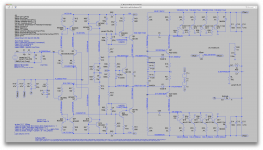
Here is what it looks like with the values I mentioned.
I set the bias and upped the trimmers on the drivers without trying to balance out, just tried getting closer to 30mA driver bias, but can't reach it.
It's not that much above, but above target, a little.
And by the way, the power dissipation in the vas trans goes down a bit below 350mw, and this probably wouldn't need heatsinking, or not much.
Attachments
Last edited:
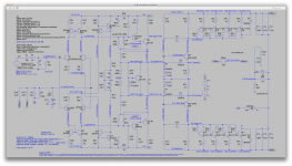
Here is something more to ponder.
I tried a little compensation tweaking, with values that seem to go a little high, with 100p on the miller and global feedback.
And just to see how it fares, I tried including the vas buffers in the miller comp.
This improves only slightly the small hint of oscillation.
Those little notches at each peaks seem to be only remnants of oscillation, nothing more.
Upping the cap values to 3n3 on the drivers brings this down more, but they don't disappear.
I left the tian probe in place so I could take a quick look at what happens to the phase margin, and at some point I brought it up to a little over 66 degrees.
Probably not necessary to be that much, but a part of that can be sacrificed to reach better thd.
Right now one goal is preventing all oscillations.
Attachments
Reading your discussions and elaborations with great interest (but with some lack of understanding, to be honest), I congrat you for managing the centering issue by bringing in R13 and R16, thus relating the rails w.r.t. gnd via the input section. After that, do you really need R46/R47 and their connection to in+? And what's the use of the chain across the Vbe multiplier, consisting of D3, D4 and both the trimpots? Sorry for jumping in, but still with best regards!
Wont R13 and R16 couple supply noise (ripple etc) directly into the feedback node ?
Might be a good concern! Read:
...And they even have a trimmer there, but it's not dc coupled, so I'm puzzled as to what it real use is....
The real use of this trimmer, called HUM NUL in the QSC schematics, very probably is to cancel hum noise.
What does LTSpice tell you on this matter?
Best regards!
If the low voltage rails are clean and stable then ripple doesn't seem to be a massive issue (I just tried it in LT but using the circuit a few posts above this). Even with ripple as high as 5 volts pk/pk on the main supply voltage and the output only had around 15mv pk/pk at most. If the low supply rails are clean then I don't see the need for a hum adjustment tbh.
Kay Pirinha asked: do you really need R46/R47 and their connection to in+? And what's the use of the chain across the Vbe multiplier, consisting of D3, D4 and both the trimpots?
Good questions, you found some puzzles in the design. There are historical reasons for those oddments. Background: We started this analysis to aid in simulating a known working commercial amp design. It used grounded collector output stage, which had great cooling advantages. But it was difficult to see how the output stage centered itself. In the end, after quite a bit of effort we found a solution. Before we found that, we tried other solutions; these are remnants of them. We'll keep them for now, because the design is finally behaving reasonably, and changes seem to have unintended consequences.
To explain why these oddments exist, I'll summarize the development. In brief, this output stage was difficult to force to a centered operating condition. It tended to saturate positive or negative and we tried many ways to tame it. You found two.
R46/R47: These force the front end output to center. These waste some gain to do this, but it proved necessary. The input stage tended to saturate positive or negative, impossible to correct without this network. (To answer your question, yes, we may revisit this as you suggest, but with caution. This design is slippery and it would be easy to destabilize it.)
Regarding your other question, why the odd network on the Vbe multiplier, the answer is to balance the two halves of output stage. The network is at the input of the output stage and it sets a similar DC operating point for each half. Without this network, when we close the global feedback loop, we do get a very nice low offset voltage at the output, that's good, but we also get a horribly uncentered floating supply voltages, not good at all. The voltage swing is limited in this state. So we add this local DC feedback, which equalizes both halves.
With the input network consisting of a high value resistor to Vfloat, the diode and resistor to ground, we are using predictably accurate resistors and negative feedback to compensate for predictably unmatched transistor parameters and floating DC. It is just an approximate centering to bring it into range, and the front end can do the rest.
I put in trimpots in the network because the R value is somewhat critical, and it's difficult to compute with many variables. Here I communicate to Spiceman Extraordinaire (Spookydd) that the resistors should be tuned from the model. To determine this R, vary R to obtain output devices' quiescent current of about 50ma using the Spice model. It's not that simple, because the Vbe multiplier interacts with the network so this we approach with caution.
I hope that explains the initial reasoning, and our caution in making changes. This journey is not over. When we improve stability to acceptable levels and have distortion lower, we can revisit some of these areas.
The notch on the top of the sine wave concerns me. How can we probe to find it's source? My hunch is it's in the output stage. But how to localize?
Since it is symmetric, we could selectively alter components on the high or low sides and see if the amplitude/shape changes. It occurs on a phase reversal, so that suggests a storage mechanism. As a first suggestion, imbalance the "miller caps" on the drivers. Make one half or twice as large, or 10x, just to see if the notch changes. If that yields nothing, then do other changes to purposely imbalance the output stage. It's just a way to localize, based on hunches. Does it make sense?
I do note one significant difference from QSC's design. They are using small caps to bypass the driver emitter resistors. This can only affect high frequencies, so I figured with our oversized Miller caps there it would do nothing and skipped it. But I'm not so sure. This is another component to add selectively, to see notch changes.
3 Experiments to try independently:
1. Cascode the VAS to isolate from load, make VAS Miller comp effective.
2. Tweak Driver feedback resistor to high value 100k.
3. Add 2n2 emitter bypass caps to drivers, purely experimental.
1. Cascode the VAS to isolate from load, make VAS Miller comp effective.
2. Tweak Driver feedback resistor to high value 100k.
3. Add 2n2 emitter bypass caps to drivers, purely experimental.
Attachments

any thought to:
1. separate into 2 blocks: input block and output block,
2. understand, characterize and optimize each individually, perhaps with it's own local NFB.
3. combine and characterize without overall NFB
4. add overall negative feedback if needed - characterize, tune and optimize?
i didn't read all the details yet of everything that's been done so far, but it seems there's a little shooting in the dark going on.
by the way, the early boulder amps (for example, 500AE) used output stages with gain. they were good sounding amps that as I recall, were pretty robust, and earned respect in high enders' homes, in studios and on the road. their philosophy didn't respect the "legend" that output stages with gain are trouble. but it does seem that they spent considerable effort carefully and rigorously studying performance capability, stability and compensation to get a "good" balance. the front end was based on the old 990 discrete op amp. might be worth digging into ...
best regards,
mlloyd1
mlloyd1 said: any thought to:
1. separate into 2 blocks: input block and output block,
2. understand, characterize and optimize each individually, perhaps with it's own local NFB.
3. combine and characterize without overall NFB
4. add overall negative feedback if needed - characterize, tune and optimize?
i didn't read all the details yet of everything that's been done so far, but it seems there's a little shooting in the dark going on.
++++++++++++++++++
I say:
The goal of this effort was to simulate this type of amp, grounded collector. The original poster was unable to make it work in simulation, but it was in production and known to work.
What was missing from the model?
Through many iterations we rediscovered the key and what to do to make it work. So, mission accomplished, original goal met.
Is this a good amp to build? We don't know yet. More tuning required to firm up stability. If it has good performance, this should be more compact than other Class AB amps, due to smaller heatsink.
It has also been an interesting challenge. The journey is the reward, perhaps?
To answer your questions:
1. Yes, this was developed as a whole, then split to analyze front and back ends separately, then recombined. The recombining was difficult, but we seem to have a good solution to issues raised.
2. Yes, input and output sections analyzed separately, many avenues explored.
3. No, it won't work well without global feedback, but we have analyzed it without, for local optimization. The necessary feedback from the output is the average or sum of the two Vfloats, which is necessary for DC and AC operation of the combined front and back ends.
4. Global NFB is necessary to avoid saturation of output.
Thanks for taking a look, and any suggestions are most welcome!
After that, do you really need R46/R47 and their connection to in+?
While we went through the many ways we could control the rail centering, many things were tried, some stayed, some were removed later. The local feedback concept can be a good thing to linearize a stage and moderately reducing gain in each stage makes for a lower amount of global feedback.
This was put forward by Matti Otala in the 70s, who I think was the first to bring up the subjet of TIM, and one of his methods to reduce the TIM was to reduce the gain in stages and then apply less feedback globally.
In this case, it wasn't the hunt for TIM that was the motivator but rather to find ways to balance the circuit to center the rail.
And what's the use of the chain across the Vbe multiplier, consisting of D3, D4 and both the trimpots? Sorry for jumping in, but still with best regards!
That too is part of the quest for a balance, and at the same time control the bias in the drivers and provide some means to correct centering.
One other aspect is addressing reverse voltages when rails swing.
Please do jump in. This is a forum and we're openly discussing things. All input are welcome.
Wont R13 and R16 couple supply noise (ripple etc) directly into the feedback node ?
If my understanding is more or less correct, since the power supply makes the rails from a single winding and followed by a bridge with no center tap, wouldn't the rippling on each rail be cancelling each other?
Perhaps the only part to worry a little more about would be the drooping from the modulation pulling current out.
The voltage swing is limited in this state. So we add this local DC feedback, which equalizes both halves.
One thing that we face in a real practical build is the differences in the npn/pnp parts, which we can mostly correct with such things. Even if we do parts matching to minimize this, it always remains more difficult to match the npn to the pnp.
The real use of this trimmer, called HUM NUL in the QSC schematics, very probably is to cancel hum noise.
I think the "hum" should be looked at differently from ripple and noise.
I think the hum is more of a grounding issue than anything else, due to interactions with other things in a system, and not just inherent in the power amp by itself.
Whatever they meant by hum, may not be related to this type of "disturbance".
I still don't see how it works. Maybe someone can shed some light on this. It should be interesting.
What does LTSpice tell you on this matter?
So far we've been battling the centering, and now that this is tamed, we're ironing out some other details but mostly still at dc and not venturing much yet into the transient area.
Besides, if we take "hum" as something coming from "outside" of the amp itself, caused by some wiring and improper grounding (loops), then spice can't tell us much about that, unless we add some virtual circuitry to the amp to simulate influences from the outside...
If the low voltage rails are clean and stable then ripple doesn't seem to be a massive issue (I just tried it in LT but using the circuit a few posts above this). Even with ripple as high as 5 volts pk/pk on the main supply voltage and the output only had around 15mv pk/pk at most. If the low supply rails are clean then I don't see the need for a hum adjustment tbh.
I'm interested in how you simulated this. Can you show us please?
Your centering scheme was interesting as well, and I'd like to know more about how this works, and how it fares when modulation is applied.
The notch on the top of the sine wave concerns me. How can we probe to find it's source? My hunch is it's in the output stage. But how to localize?
I've been experimenting quite a bit around this, and trying to eliminate it with the compensation. During my explorations, I got the feeling that this was originating in the vas and not the output stages.
The global feedback comp could not completely eliminate it, with the action of the compensation on the drivers, which was very limited, and the miller caps, all combined, could not completely get rid of that little notch issue.
While tweaking values, I saw that in fact that notch seemed to be more of a left over oscillation that was mostly eliminated but not completely.
Then going on a hunch that the source was in the vas, I tried adding a comp cap on the 2n440x emitters, and tweaked the value so that notch was totally gone, and I got a phase margin of over 50 degrees then, with the thd not really satisfactory at nearly 0.2%.
A bit more tweaking of all the compensation got the phase margin up to about 55-56 degrees and thd down to just about 0.1%.
Better, but could be better.
The most effective compensation was the one added on the 2n440x emitters. Once there and the value adjusted, I was able to drop the values on the other comp caps, which was the main cause of dropping thd from about 0.2 to 0.1%.
All that while keeping a phase margin at well over 50 degrees.
Now I may be wrong with some of it. Because I am not 100% certain to be using the loop gain probe exactly right for this topology, because of its output configuration, I think I could be missing something.
The reason that makes me think this is although the phase margin reads right, the gain margin is totally wrong, big time, giving a large negative value.
So I think this should be solved before relying on those particular measurements.
Since it is symmetric, we could selectively alter components on the high or low sides and see if the amplitude/shape changes. It occurs on a phase reversal, so that suggests a storage mechanism. As a first suggestion, imbalance the "miller caps" on the drivers. Make one half or twice as large, or 10x, just to see if the notch changes.
I can try that, but if my use of the caps on the emitters is of any help, perhaps we know more or less what those notches are now.
If that yields nothing, then do other changes to purposely imbalance the output stage. It's just a way to localize, based on hunches. Does it make sense?
Maybe I already found out, but I'll try this stuff to see what happens.
I do note one significant difference from QSC's design. They are using small caps to bypass the driver emitter resistors. This can only affect high frequencies, so I figured with our oversized Miller caps there it would do nothing and skipped it. But I'm not so sure. This is another component to add selectively, to see notch changes.
I did try experimenting with caps there earlier. And they did a lot to stabilize it, and eliminate oscillations. Very effective, but at the cost of degraded phase margin at the time, and it also caused a huge increase in that gain spike around the 1-2mhz. It has a strong effect and brings side effects, so this should be used with great caution. Perhaps calculations would determine a range of values, to stay within, and the tweaking within that range, but not going beyond it...
I have one big question for those who are well versed in using the loop gain probe (tian's method). If I understand this right, because mostly of topology and the fact that the global feedback tap is taken before the output coil and not right at the speaker output, that coil and the zobel if it's placed on the speaker side as well, are excluded from the loop while measuring the phase and gain margins.
And so is the amp's input network, which also excludes the input filter.
Is this right?
Are we only considering the in+/in- as the amp's input, directly only?
And excluding the output coil?
qsc places the zobel on the speaker side and not the amp's output side, so placed that way, the zobel is also out of the main loop and not considered in phase/gain margin.
I want to grasp this better, but it's not really that easy. The only examples I've seen that show how to use the tian loop probe are opamp based, and it's not always that easy to transpose this in a discrete topo.
Help please.
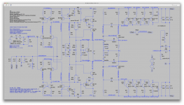
3 Experiments to try independently:
1. Cascode the VAS to isolate from load, make VAS Miller comp effective.
Ok, I'm about to try this out now.
3. Add 2n2 emitter bypass caps to drivers, purely experimental.
I did try that before, as I mentioned earlier. With great effect, and side effects. To be tamed and used properly.
It does have potential and perhaps could allow eliminating the caps on the driver's cb, which aren't very effective anyway and can only bring in more thd, and perhaps other side effects of their own, in regards to little positive effect.
From experimenting, it seems to me that using caps there (driver emitters) and on the vas emitters (the 2n440x), was much more effective at curbing oscillations than having them on the driver's cb.
The caps on the drivers may even probably not be needed at all, if the one on the vas emitters are enough to curb oscillations.
The less caps are used, the better...
3 Experiments to try independently:
1. Cascode the VAS to isolate from load, make VAS Miller comp effective.
2. Tweak Driver feedback resistor to high value 100k.
3. Add 2n2 emitter bypass caps to drivers, purely experimental.
Oh, and by the way, while looking at where you're tapping the cascode vas bases, that reminds me of one other experiment that I conducted.
I thought that since the ltp current sources are symmetric and complementary, they could be unified more to prevent the small imbalance that we have there.
The divider network of 47k res with their middle tap to ground are allowing a slightly different current to be driving those sources. Not a big difference, but in a differential stage, every small value has a good amount of effect.
So I figured, instead of 4 resistors, with a middle tap to ground, we could simplify that to a single resistor, with nothing to ground, and thus both current sources would forcibly have the same tail current.
So instead of the 4 47k res, I put a single 220k there, which does slightly reduce that tail current, for about 200uV, which actually changes nothing to the ltp tail current sourced, so no adverse effect.
One positive effect of forcing this same tail current on the sources, is that the ltp tail currents are much closer to each other, with each branch in the ltp more balanced.
And one other small detail that I did observe when doing this, was that thd went down a little as well.
I did try that during the experimentation with the comp caps, when I got all signs of oscillations disappear with the use of the vas emitter caps.
Just something more to ponder. This brings down the part count, while actually improving the whole thing...
3 Experiments to try independently:
1. Cascode the VAS to isolate from load, make VAS Miller comp effective.
Before going on to the next steps, here are some snapshots of what we get by adding the cascodes.
I didn't try to adjust any compensation and didn't touch the driver base trimmers.
I only added the cascodes and trimmed for proper bias.
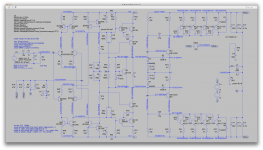
I did try it with the 47k divider before moving on the the 10k, so the currents could be compared.
Do we need that much tail current in the current sources?
Going to 10k also increses a little the ltp tail current, so each branch is now close to 3mA.
About my idea of combining the divider res in the sources tails into one. This wouldn't work if we need a tap for the cascodes, but perhaps it is still possible to combined the 2 in the middle and get off the ground tap. Perhaps the 2 caps could be one on the single res in the middle...
But I'm not sure it's good to have that much more tail current there. Is this for the cascode to use?
Attachments
- Status
- Not open for further replies.
- Home
- Amplifiers
- Solid State
- grounded collector amp