......
Now, we're having an issue with the operating point.
I did get the bias correct on the outputs are close to 100mA, but we can see there is a sizeable dissymmetry.
......
We need to change R17 and R18 in your schematic to 100K, not 22K. This should center things again. This puts about 0.6v at the driver bases at idle, and sets output stage DC gain near 100.
I did a variation using MOSFET drivers. There is a hazard with the bipolar drivers, of reverse biasing the base-emitter junctions to destruction. Limiting drive voltage from the input stage avoids this. But MOSFETs don't care, so I tried them. Simpler.
Attachments
Last edited:
We need to change R17 and R18 in your schematic to 100K, not 22K. This should center things again. This puts about 0.6v at the driver bases at idle, and sets output stage DC gain near 100.
It didn't go that way.
Now it's almost pegged all the way to the high rail. Something else is amiss.
I did a variation using MOSFET drivers. There is a hazard with the bipolar drivers, of reverse biasing the base-emitter junctions to destruction. Limiting drive voltage from the input stage avoids this. But MOSFETs don't care, so I tried them. Simpler.
We can try that next, but can we fix this last one?
We'll have an opamp and mosfet based one to do as well.
Which will work best, we'll see...
Attachments
It didn't go that way.
Now it's almost pegged all the way to the high rail. Something else is amiss.
We can try that next, but can we fix this last one?
.
Swap the inputs to the diff pair. You've been battling positive feedback the whole time.
Swap the inputs to the diff pair. You've been battling positive feedback the whole time.
Revised schematics attached.
Attachments
Swap the inputs to the diff pair. You've been battling positive feedback the whole time.
Wow! Good catch. I didn't even see that.
Revised schematics attached.
Doing it one at a time. Otherwise too confusing.
Even after swapping the diff inputs, and updating the various values and other details, it still wants to swing all the way up.
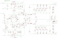
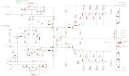
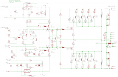
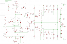
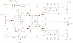
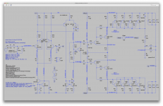
I separated the output stages again between the vas and drivers, keeping the bias spreader in place or it wouldn't work, and we can see the output stages are fairly well balanced, which I think it mostly due to those dividers of 100/1k on each driver's bases, but the part that is way out of balance is the bias spreader, pulling down almost all the way to its own low rail.
When connected to the rest, it comes back mostly to center, but obviously not enough and the whole thing swings all the way up.
Curiously, the bias is adjustable and despite the swing all the way up, it's able to be set at about 100mA fairly evenly.
Attachments

On this one, I used the bat54 from the ltspice library, as I didn't have the bas40 model handy, but that shouldn't affect it would it?
Anyway, although the imbalance is much less, the rails still aren't centered and the bias can't be adjusted.
I would like to know if the ferrite beads can be simulated. Seeking input from the gurus out there...
Anyway, although the imbalance is much less, the rails still aren't centered and the bias can't be adjusted.
I would like to know if the ferrite beads can be simulated. Seeking input from the gurus out there...
Attachments
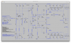
Tried out the mosfet version.
It is less imbalanced than the bjt, but rails not centered.
I could adjust the bias to 100mA, and ran a transient analysis, which took a long time, because we have significant oscillations.
I used a model for the irf9640 that was in the ltspice lib, but didn't have its counterpart irf640 there, so I dug out an other model for that, and perhaps they are too dissimilar..
If someone has a good pair of models for those mosfets, I'd like to try them, otherwise perhaps we can pick something in the ltspice lib.
Attachments
And spooky - I don't see the 'grounds' connected to your supposedly grounded collectors. You'll be running off the drivers, and in a real circuit they'd get pretty toasty.
Frequency compensation will probably be a real sob, but it always is until you figure a topology out for the first time.
Frequency compensation will probably be a real sob, but it always is until you figure a topology out for the first time.
And spooky - I don't see the 'grounds' connected to your supposedly grounded collectors. You'll be running off the drivers, and in a real circuit they'd get pretty toasty.
You didn't notice them, but they're there.
I know I could pull them out to be seen better. It's when I moved things around early on, it was stuck right on the node and I just left them that way.
Frequency compensation will probably be a real sob, but it always is until you figure a topology out for the first time.
At least we can see how the big guys did it.
I'm wondering about the grounding for those grounded collector schemes.
Since all the output devices have their collectors directly connected to the heatsinks, they're automatically at the chassis, so what about ground loops?
What is there to watch out for as far as the other ground connections are concerned?
Of course doing some ground lifting for the signal ground and things like that can help, but then having the ground all around in the chassis with different parts of the amp connected to different points makes it tricky.
Doing it one at a time. Otherwise too confusing.
Even after swapping the diff inputs, and updating the various values and other details, it still wants to swing all the way up.
I separated the output stages again between the vas and drivers, keeping the bias spreader in place or it wouldn't work, and we can see the output stages are fairly well balanced, which I think it mostly due to those dividers of 100/1k on each driver's bases, but the part that is way out of balance is the bias spreader, pulling down almost all the way to its own low rail.
When connected to the rest, it comes back mostly to center, but obviously not enough and the whole thing swings all the way up.
Curiously, the bias is adjustable and despite the swing all the way up, it's able to be set at about 100mA fairly evenly.
Once again, Spice reveals all. This won't center due to component values being low.
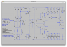
The output stage must center by itself, but the predrivers are not turned on enough to do that. I changed the centering divider, adding diodes and a pot which should provide slightly higher voltage, and a centering adjust all in one. Incidentally, this may be the elusive secret to QSC centering, I suspect. I chose the pot as 500 ohm initially, which may be too high or low so you'll change it as needed. We want to end up with about 30ma into R27 and R28, or 100ma in all outputs. The bias spreader voltage may need to increase slightly also to match whatever voltage we see at the inputs to the disconnected front end. But that interacts with many things, so that's just my hunch.
To address a different concern, I added two 1.5k resistors which reduce the drive voltage, to protect the predriver base-emitter junctions from destructive reverse voltage if overdriven extremely. It could be destructive and puts the transistor in a strange mode. This could have side effects, so it's tentative.
Lastly, as an experiment I suggest removing the DC blocking caps from the feedback divider. This should force DC centering, but will result in slightly higher DC offset at the output. Explore this after the divider net is working. As you recall, QSC had the DC blocking caps, but a 1.6k resistor to ground at the center of the feedback divider, so it's much the same. They probably wanted to reduce DC offset, but keep DC centering, conflicting objectives. See how that goes.
Attachments
On this one, I used the bat54 from the ltspice library, as I didn't have the bas40 model handy, but that shouldn't affect it would it?
Anyway, although the imbalance is much less, the rails still aren't centered and the bias can't be adjusted.
I would like to know if the ferrite beads can be simulated. Seeking input from the gurus out there...
Any schottky diode is fine. I think I will not develop this further because a simple resistive divider probably works about as well to protect the base-emitter junction of the predriver.
Ferrite beads are lossy inductors. Would it make sense to model them as a very small resistor in series with an inductor? Not my expertise. Murata specs different ones as having 22-1000 ohm reactance at 100MHz. You can reverse engineer the inductance from that and DC resistance under 1 ohm. Other vendors tell you the inductance.
Anyway they are very effective at MOSFET gates to squelch oscillation. We seem to have a case of that in a later design. Not surprised, that's what they like to do. Might have to use RC filters too.
You can try to add some local feedback around the output stage. From the NFB point to the emitter of Q12, and 13. This will gives better performance for the output stage.
Sajti
Sajti
I'm wondering about the grounding for those grounded collector schemes.
Since all the output devices have their collectors directly connected to the heatsinks, they're automatically at the chassis, so what about ground loops?
What is there to watch out for as far as the other ground connections are concerned?
Of course doing some ground lifting for the signal ground and things like that can help, but then having the ground all around in the chassis with different parts of the amp connected to different points makes it tricky.
We'll have ground loops on the outputs. With the collectors screwed bare to the heatsinks, and multiple devices, we can't avoid them. It's OK. The trick is to split the input section ground away from the output section ground or grounds, and return it to the star ground separately. Physical layout and wiring matter a lot, even though they don't show on the schematic or the model. On card, the routing of the feedback line matters greatly too. There are many details like that.
That's a whole separate discussion that merits deep thought, depending on your design and packaging so much.
The output stage must center by itself, but the predrivers are not turned on enough to do that. I changed the centering divider, adding diodes and a pot which should provide slightly higher voltage, and a centering adjust all in one. Incidentally, this may be the elusive secret to QSC centering, I suspect. I chose the pot as 500 ohm initially, which may be too high or low so you'll change it as needed. We want to end up with about 30ma into R27 and R28, or 100ma in all outputs. The bias spreader voltage may need to increase slightly also to match whatever voltage we see at the inputs to the disconnected front end. But that interacts with many things, so that's just my hunch.
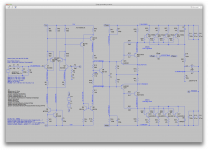
Ok, with everything in place (except taking out the caps on the feedback), the rails still fly way up there close to the high side, so I split it again to look at each part's behavior.
As you can see on the screenshot, I ended up keeping that centering pot to 500ohms, as lowering it would take out some current and make centering more tricky. Increasing its value brings up a little much bias current, and we don't even have the bias spreader hooked up yet...
With the 2 parts isolated, I can center the output part about alright and we have some 10mA of bias in each output already. Maybe a bit much...
To address a different concern, I added two 1.5k resistors which reduce the drive voltage, to protect the predriver base-emitter junctions from destructive reverse voltage if overdriven extremely. It could be destructive and puts the transistor in a strange mode. This could have side effects, so it's tentative.
Ok, we'll see what that does when we reconnect everything, but for now, the front end part is the one causing the imbalance.
With the caps still in the feedback network, we can see the imbalance, as it's pulling down.
Lastly, as an experiment I suggest removing the DC blocking caps from the feedback divider.
With the caps taken out of the way, we have about the same drift but in the other direction. (2nd screenshot)
This should force DC centering, but will result in slightly higher DC offset at the output.
I don't think we have much to worry about any dc offset on the speaker output. There is no way it can come out even when the rails are all the way pulled in either direction. We have those big filter caps that are blocking any possible dc.
If you look again at earlier attempts, when it was pulling all the way up to the plus side rail, we still had hardly any dc on the output and I suspect it was more coming from the feedback from the front end...
If we can get the front part to self center better, I think we're on to something...
Attachments
You can try to add some local feedback around the output stage. From the NFB point to the emitter of Q12, and 13. This will gives better performance for the output stage.
Sajti
In the refinement stage, we'll explore stuff like that. Right now, it's grossly broken. We need to get the output stage to turn on and center at idle, before going to the next area. That's top of the list.
Ferrite beads are lossy inductors. Would it make sense to model them as a very small resistor in series with an inductor?
Maybe, if we use a very small value resistor, and if we know what inductor value to add in series, that may do the trick.
The trick is to split the input section ground away from the output section ground or grounds, and return it to the star ground separately.
That can be done, but we don't have a total star config possible with those spread out grounds to chassis.
Physical layout and wiring matter a lot, even though they don't show on the schematic or the model. On card, the routing of the feedback line matters greatly too. There are many details like that.
And that's the part that I thought could not really be properly simulated.
That's a whole separate discussion that merits deep thought, depending on your design and packaging so much.
Yep, and I'm sure we'll have a few gurus having something to contribute on that.
- Status
- Not open for further replies.
- Home
- Amplifiers
- Solid State
- grounded collector amp