where I aim for 50ma per output roughly, not critical. We're close, but showing crossover, so that may need to be 100ma per.
That's roughly what I usually try to aim for, or perhaps sometimes up to 150mA or a little more.
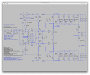
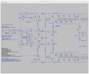
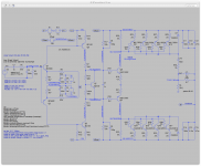
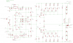
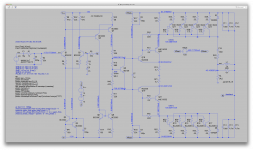
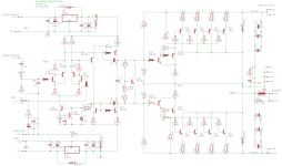
The extreme comparator behavior must end. We can reduce the gain of the front end, by removing the complementary Darlington transistors, or adding local feedback, or both. I show both in the schematic below. If it is easy, I'd like to know the effect of each change independently. Try the local feedback via the 270k resistors alone.
Alright, let's see if we just add that extra local feedback, keeping the darlingtons...
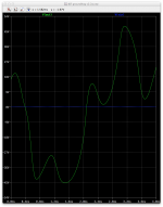
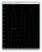
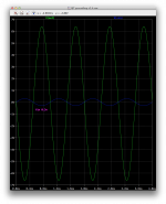
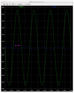
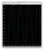
On the first version shown, I saw that a 1V input signal was sending it way into clipping, so I reduced that and what comes out isn't so pretty.
Then I increased the signal a bit and it does exhibit some comparator behavior still, but not as much as before.
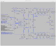
Try removing the complementary transistors in the first stage alone. Try both together. If you do only one, do the last.
Let's try that next.
Attachments
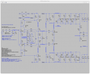
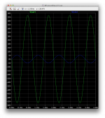
Try removing the complementary transistors in the first stage alone.
With the extra trannies removed.
Both local and global feedback.
No adjustment of bias, but it's enough that if it worked right it wouldn't be too bad as is.
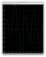
Much less crossover distortion already.
Still not so pretty though.
Attachments
Try removing the complementary transistors in the first stage alone. Try both together. If you do only one, do the last.
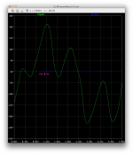
Now without the local feedback, and the extra trannies.
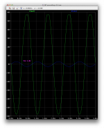
The local feedback doesn't seem to bring much.
There are stability risks with nested feedback so this is a critical analysis. It is so incredibly useful to have this modeling.
Far faster than breadboarding.
Once it works nicely in sim, then time to move on to breadboard...
Attachments

The reason you're having trouble with this, and why qsc uses an op amp is because the output stage is inverting. The ground and speaker out are swapped, so it needs an inverting front end. Look at the qsc schematic, and see which pin the signal goes in, and which the feedback goes in.
Good point!
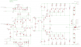
You are correct. The negative feedback should be applied directly to the input node. A modified schematic follows.
Right.
Here we go. Much better already.
Looks mostly "normal" with a small input signal, although we can now see it's an inverting amp.
With a larger input, the comparator behavior is gone, and I pushed it a bit beyond its limit, to see how it clips, and we can see it's uneven, and the offset on the output is tiny, so it's not the cause.
Before clipping occurs, I saw distortion in the order of 1%.
It's getting there...
Attachments
Adjusting the bias to about 100mA took the bias trimmer to 529ohms.
I only look at one of the output devices' current, but they should all be fairly close, and we can confirm by looking at the total idle current from the supply.
It takes a 2.6v input to bring it close to the onset of clipping, which still occurs at the high rail first.
At that level, we get close to 1.5% thd.
Although it is now inverting, I see less phase shift though.
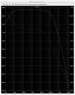
ac analysis shows it tends to cut a little high at the low end of the spectrum.
At the high end of it, it seems fairly reasonable, but probably could be better.
I only look at one of the output devices' current, but they should all be fairly close, and we can confirm by looking at the total idle current from the supply.
It takes a 2.6v input to bring it close to the onset of clipping, which still occurs at the high rail first.
At that level, we get close to 1.5% thd.
Although it is now inverting, I see less phase shift though.
ac analysis shows it tends to cut a little high at the low end of the spectrum.
At the high end of it, it seems fairly reasonable, but probably could be better.
Attachments

Quite flawed, but it zeroes
You are absolutely correct. My last change was with great reservation. I don't like it, but it was a rescue of a fatally flawed design. Trying to make the front end with 4 discrete transistors was a self-imposed challenge, with many compromises. You point out one of many limitations. I made a self imposed goal to keep it ultra simple, but this became too primitive for good performance. Of course I can add a more elaborate front end using more discretes that works better. However, is that practical? I suppose that is a judgement call, but for me an op amp based design like the original QSC and my post 47 just makes so much more sense for this topology.
Do remember that the our purpose is not to design an amp, but to simulate the QSC style of grounded collector amp with its floating power voltages. Obviously, it works in the production amps, but it's apparently hard to model. In particular, how does the grounded collector amp establish ground with those floating power voltages? I had a paper design sitting around which was easy to model and did zero nicely, and as we know had a design oversight, now crudely patched. Hopefully it helped understand the simulation better, my main purpose.
The novelty of the QSC design is the grounded collectors, which has cooling benefits. The output devices can be directly mounted to a heat sink without insulators, greatly reducing thermal resistance to 1/3 of the resistance with any insulator. Lowering thermal resistance this is very significant. On a high powered Class AB amp, it allows much smaller heatsinks. I have a Hafler DH500 that is comparable in power out, but twice the size and weight of a QSC1700. That is a graphic example of the benefits of the QSC approach. It is targeted at commercial PA uses like cinemas, where people use multiple high powered amps and where savings in size and weight help sell products. Performance is acceptable for that market, not for the audiophile market I think.
Hi Slowhands,
You have to take in account that if AC signal source at the input is low impedance (most of them are low enough), R1+R9 appear connected in parallel with R2. So the feedback ratio is very different from what you expected (overall gain is pretty much higher). Influence of R2 here is rather low in gain equation, assuming its high value, comparing to R1+R9.
Cheers,
Valery
You are absolutely correct. My last change was with great reservation. I don't like it, but it was a rescue of a fatally flawed design. Trying to make the front end with 4 discrete transistors was a self-imposed challenge, with many compromises. You point out one of many limitations. I made a self imposed goal to keep it ultra simple, but this became too primitive for good performance. Of course I can add a more elaborate front end using more discretes that works better. However, is that practical? I suppose that is a judgement call, but for me an op amp based design like the original QSC and my post 47 just makes so much more sense for this topology.
Do remember that the our purpose is not to design an amp, but to simulate the QSC style of grounded collector amp with its floating power voltages. Obviously, it works in the production amps, but it's apparently hard to model. In particular, how does the grounded collector amp establish ground with those floating power voltages? I had a paper design sitting around which was easy to model and did zero nicely, and as we know had a design oversight, now crudely patched. Hopefully it helped understand the simulation better, my main purpose.
The novelty of the QSC design is the grounded collectors, which has cooling benefits. The output devices can be directly mounted to a heat sink without insulators, greatly reducing thermal resistance to 1/3 of the resistance with any insulator. Lowering thermal resistance this is very significant. On a high powered Class AB amp, it allows much smaller heatsinks. I have a Hafler DH500 that is comparable in power out, but twice the size and weight of a QSC1700. That is a graphic example of the benefits of the QSC approach. It is targeted at commercial PA uses like cinemas, where people use multiple high powered amps and where savings in size and weight help sell products. Performance is acceptable for that market, not for the audiophile market I think.
Adjusting the bias to about 100mA took the bias trimmer to 529ohms.
I only look at one of the output devices' current, but they should all be fairly close, and we can confirm by looking at the total idle current from the supply.
It takes a 2.6v input to bring it close to the onset of clipping, which still occurs at the high rail first.
At that level, we get close to 1.5% thd.
Although it is now inverting, I see less phase shift though.
ac analysis shows it tends to cut a little high at the low end of the spectrum.
At the high end of it, it seems fairly reasonable, but probably could be better.
Good, apparently this is at least functional. Now, how do we keep it simple, but reduce distortion. The front end seems balanced, the output not so much. Perhaps more gain will help. We can add a Darlington gain stage to the output, and the input as before. Valery made a good point about the source impedance affecting the feedback ratio, so I tweaked the input filter, reducing sensitivity in the process. I increased the input capacitor based on your comment.
Attachments
Good, apparently this is at least functional.
Yes, defintely much better. We're on track.
Now, how do we keep it simple, but reduce distortion.
Well, it can remain simple and yet have a few more parts, it's no big deal to add a few parts if the benefits are real and significant.
The front end seems balanced, the output not so much. Perhaps more gain will help. We can add a Darlington gain stage to the output, and the input as before.
Why not? If it works better. And it wouldn't be that much more complex really.
Valery made a good point about the source impedance affecting the feedback ratio, so I tweaked the input filter, reducing sensitivity in the process. I increased the input capacitor based on your comment.
Alright, then we'll try this out next.
Something is wrong with the bias spreader.
It doesn't find a proper operating point.
Totally out of balance.
Is there a reason for picking up the local feedback between the bias trimmer and the 470ohm resistor (R18 on the schematic, R46 in the sim)?
This isn't the cause of the imbalance, but it likely contributes, maybe, and how can it be overall symmetric that way?
I tried separating the input stage from the rest, between the vas and drivers, keeping the bias spreader where it belongs in the vas, and it was much closer to balance, but not sure what is causing it exactly.
I added more voltages to see what's going on with the operating point. I should shed some light on this.
Attachments
Something is wrong with the bias spreader.
It doesn't find a proper operating point.
Totally out of balance.
Is there a reason for picking up the local feedback between the bias trimmer and the 470ohm resistor (R18 on the schematic, R46 in the sim)?
This isn't the cause of the imbalance, but it likely contributes, maybe, and how can it be overall symmetric that way?
I tried separating the input stage from the rest, between the vas and drivers, keeping the bias spreader where it belongs in the vas, and it was much closer to balance, but not sure what is causing it exactly.
I added more voltages to see what's going on with the operating point. I should shed some light on this.
Just a drafting error, I hope. The feedback was picked up at the wrong node. See schematic.
Attachments
Just a drafting error, I hope. The feedback was picked up at the wrong node. See schematic.
I figured. But fixing that still isn't helping with the biasing issue.
See the screenshots. A big imbalance and altering the bias trimmer doesn't bring it to proper operating point.
And for kicks, look at the second shot, where I deleted the links between the vas and drivers, to isolate the front end. Without that link, the bias spreader looks much closer to normal, but not the output stages.
A little more to tweak.
Attachments
I figured. But fixing that still isn't helping with the biasing issue.
See the screenshots. A big imbalance and altering the bias trimmer doesn't bring it to proper operating point.
And for kicks, look at the second shot, where I deleted the links between the vas and drivers, to isolate the front end. Without that link, the bias spreader looks much closer to normal, but not the output stages.
A little more to tweak.
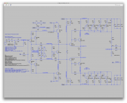
Swap the driver transistors MJ15032 and MJ15033, as in my schematic. That's probably it.
I am very unhappy with the front end compromises on input filter and feedback divider. So I put together a more conventional front end, essentially a discrete op amp front end in the below schematic. This is just a fallback, still discrete parts. I admit to being curious how it compares in performance.
Attachments

Swap the driver transistors MJ15032 and MJ15033, as in my schematic. That's probably it.
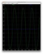
It was. And for the first time we now get a good looking sine wave coming out, and a far more decent distortion result:
Fourier components of V(out)
DC component:0.00922793
Harmonic Frequency Fourier Normalized Phase Normalized
Number [Hz] Component Component [degree] Phase [deg]
1 1.000e+3 5.707e+1 1.000e+0 179.24° 0.00°
2 2.000e+3 3.648e-2 6.392e-4 81.52° -97.73°
3 3.000e+3 1.004e-1 1.759e-3 -167.42° -346.66°
4 4.000e+3 4.716e-2 8.263e-4 89.79° -89.45°
5 5.000e+3 2.784e-2 4.878e-4 156.02° -23.22°
6 6.000e+3 1.799e-2 3.151e-4 88.07° -91.17°
7 7.000e+3 3.241e-2 5.680e-4 -174.90° -354.14°
8 8.000e+3 1.960e-3 3.435e-5 91.71° -87.53°
9 9.000e+3 5.201e-3 9.113e-5 144.48° -34.76°
Total Harmonic Distortion: 0.220355%(0.223063%)
Clipping is nice, even and smooth, although the input network dividing the signal loses a lot of it and the overall gain isn't that high, so it take 5v peak to bring it at the onset of clipping.
It is inverting.
Working nicely though.
I am very unhappy with the front end compromises on input filter and feedback divider. So I put together a more conventional front end, essentially a discrete op amp front end in the below schematic. This is just a fallback, still discrete parts. I admit to being curious how it compares in performance.
Me too, I will work on that one next.
It's interesting to see it working, and for once, we got a grounded collector simulation that does work.
I just corrected this last v2.5 to make it work. If someone is interested in getting the sim files, I can post them, or we can just move on to the next best thing...
Attachments
Outstanding simulation work. Finally this model simulates well and seems to have acceptable performance for PA work. It seems to lock on ground well. I think the QSC models must have some similar but less obvious mechanism to center ground, probably the op amp supply resistors.
I feel that now that this is stable, there is an opportunity to tune it. The HF rolloff on the driver is rather extreme, a first cut for stability but not optimal. The fixed gain in the front end may be a waste, and the fixed gain in the output may be too low. Those are some variables that I'm curious about. Nothing is urgent though, I'm relieved this settled down.
Many thanks for shedding light on this, and I will look forward to any future simulations.
Finally this model simulates well and seems to have acceptable performance for PA work. It seems to lock on ground well. I think the QSC models must have some similar but less obvious mechanism to center ground, probably the op amp supply resistors.
Something I'm definitely missing and none of those simulations managed to center properly.
With a little tweaking, this v2.5 should be working pretty well and the distortion could get a little better. Remains to be seen how it performs in other areas, and then the muting and other things can then be looked at.
I feel that now that this is stable, there is an opportunity to tune it. The HF rolloff on the driver is rather extreme, a first cut for stability but not optimal. The fixed gain in the front end may be a waste, and the fixed gain in the output may be too low. Those are some variables that I'm curious about. Nothing is urgent though, I'm relieved this settled down.
Well for once it's nice to finally have one of those simulating properly.
And in discrete form, which I favor.
Now we can tune some more...
I put together the v2.7 and found a mistake in the front end current source. Q2 in your schematic was the wrong type and turned the wrong way.
Once swapped for the other type and turned back around, it started working, at least on the front end part.
Then after adjusting the bias to about 100mA per O.D., we can see something isn't quite right there. Starting from the vas we can see a dissymmetry. Although the bias currents in the outputs are rather well matched, the rails are not floating quite to center, and there is a bit high offset on the in+ at the front end.
And one other thing, isn't the current in the front end ltp a little bit "beefy"?
Attachments
....
I put together the v2.7 and found a mistake in the front end current source. Q2 in your schematic was the wrong type and turned the wrong way.
Once swapped for the other type and turned back around, it started working, at least on the front end part.
Then after adjusting the bias to about 100mA per O.D., we can see something isn't quite right there. Starting from the vas we can see a dissymmetry. Although the bias currents in the outputs are rather well matched, the rails are not floating quite to center, and there is a bit high offset on the in+ at the front end.
And one other thing, isn't the current in the front end ltp a little bit "beefy"?
Brilliant, this simulation is a tremendous aid in design.
Feedback current from the output stage is too high relative to the second stage drive current. As a fix increase the drive current so it dominates and ground reference the output stage feedback. Upgrade the second stage transistors for the higher drive current (overkill, but conservative on dissipation).
Add a Szlikai pair at the front end to make the gain higher, partly to compensate for the lower gain of the new second stage transistors but mostly because it will reduce distortion.
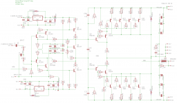
And so it goes. See schematic below.
Attachments
Last edited:
Stability problems possible
Very often I have seen this type of input stage have parasitic oscillation at the second stage driver outputs. I'm not sure why, but it is prone to it. We have to address this and prevent it cleanly. Some of it could be layout strays, we can use a ground plane and careful layout to sidestep that issue, but I don't think it's enough.
I have seen people put resistors from second stage collectors to ground, or even fairly large 330pF caps to ground there. The Symasyn amp used resistors and caps. The Hafler DH 200 and 500 used caps only. These solutions worked but seemed like a sledgehammer solution. There should be a cleaner way to quench these oscillations. As an experiment, I added ferrite beads at several locations. These are surface mount, 402 size, and cost little but may prevent this devilish problem. This is just one approach, I have other ideas. Yet another revision, but for a good cause.
Attachments
Brilliant, this simulation is a tremendous aid in design.
No contest with breadboarding.
Feedback current from the output stage is too high relative to the second stage drive current. As a fix increase the drive current so it dominates and ground reference the output stage feedback. Upgrade the second stage transistors for the higher drive current (overkill, but conservative on dissipation).
Not so much of an overkill. Those BDs are rather small signals despite their TO126 cases. We've been using them for vas in many designs.
Add a Szlikai pair at the front end to make the gain higher, partly to compensate for the lower gain of the new second stage transistors but mostly because it will reduce distortion.
I've used that too, and for a few more parts, it's often worth it.
Now, we're having an issue with the operating point.
I did get the bias correct on the outputs are close to 100mA, but we can see there is a sizeable dissymmetry.
As I mentioned before, since this topo can't pass dc, if there is an issue that would normally send big dc out to the speaker, it doesn't go there, which for pro pa can be a safety net.
Attachments
Some of it could be layout strays, we can use a ground plane and careful layout to sidestep that issue, but I don't think it's enough.
Well, that part of it can't be simulated, unless there is something I don't know.
As an experiment, I added ferrite beads at several locations. These are surface mount, 402 size, and cost little but may prevent this devilish problem. This is just one approach, I have other ideas. Yet another revision, but for a good cause.
For that I'm not sure it can be done in simulation.
This is a good opportunity to ask people to shed some light on this.
I don't know enough about spice to be sure this can be done.
- Status
- Not open for further replies.
- Home
- Amplifiers
- Solid State
- grounded collector amp