Hi
in case someone is looking for pre-build Boards of Goldmund Telos clones…
https://www.diyaudio.com/community/threads/goldmund-telos-clown-boards.395953/
Fab
in case someone is looking for pre-build Boards of Goldmund Telos clones…
https://www.diyaudio.com/community/threads/goldmund-telos-clown-boards.395953/
Fab
I had a new version, to work again 9 times. And it is my best. Because it's not as easy as we think.
If I have free time, I will share this layout design!
I am very busy, I hope to sympathize!
Some information made, thank you
1-
2-
If I have free time, I will share this layout design!
I am very busy, I hope to sympathize!
Some information made, thank you
1-
Attachments

Hello to everybody.
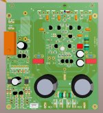
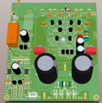
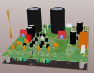
I have bought boards supposed from a Goldmund Telos 600 clone (ppower output and input boards) but I received no schematics and I really need help to make this work.
Input board:

output board:

The input board is very close to Erikovsky schematic but no caps connected to GND:

2N5565 has been replaced with U402 and I don’t know if this is a direct or any good substitute or better fit LSK389 (2sk389) or 2N3958.
I'm just building output stage and no input selector or whatever. I will use my preamp to feed the front end input board but I have some questions:
It looks obvious I have to connect input board BIAS+/-/GND with output boards BIAS+/-/GND.
Most probably I will use +/-60VDC to feed the amp and will connect regulated +/- 60VDC to the drivers (VCC+ / GND / VCC- ) and unregulated +/- 60VDC to the output mosfets VCC+/ GND / VEE-
Shall I feed +/- 60VDC to AVCC_PRE / AGND / AVEE_PRE as well?
What about feedback input? shall I connect anything there?
Will this only two boards work properly?
Thanks in advance for your help.
I have bought boards supposed from a Goldmund Telos 600 clone (ppower output and input boards) but I received no schematics and I really need help to make this work.
Input board:
output board:
The input board is very close to Erikovsky schematic but no caps connected to GND:
2N5565 has been replaced with U402 and I don’t know if this is a direct or any good substitute or better fit LSK389 (2sk389) or 2N3958.
I'm just building output stage and no input selector or whatever. I will use my preamp to feed the front end input board but I have some questions:
It looks obvious I have to connect input board BIAS+/-/GND with output boards BIAS+/-/GND.
Most probably I will use +/-60VDC to feed the amp and will connect regulated +/- 60VDC to the drivers (VCC+ / GND / VCC- ) and unregulated +/- 60VDC to the output mosfets VCC+/ GND / VEE-
Shall I feed +/- 60VDC to AVCC_PRE / AGND / AVEE_PRE as well?
What about feedback input? shall I connect anything there?
Will this only two boards work properly?
Thanks in advance for your help.
1. Siliconix U402 may directly replace 2N5565 due its same pins out. But its much lower Gm, therefore the circuit is more stable and lighter sounding. However using U402 is not good idea.
2. You can supply to front-end card, driver transistors, output MOSFETs by +/-60VDC. This is most popular way.
3. Feedback input connect to solder pad that near ''bias +/bias -'' points.
Where do you buy these boards?
2. You can supply to front-end card, driver transistors, output MOSFETs by +/-60VDC. This is most popular way.
3. Feedback input connect to solder pad that near ''bias +/bias -'' points.
Where do you buy these boards?
hello.Hello to everybody.
I have bought boards supposed from a Goldmund Telos 600 clone (ppower output and input boards) but I received no schematics and I really need help to make this work.
Input board:
View attachment 1264833
output board:
View attachment 1264832
The input board is very close to Erikovsky schematic but no caps connected to GND:
View attachment 1264837
2N5565 has been replaced with U402 and I don’t know if this is a direct or any good substitute or better fit LSK389 (2sk389) or 2N3958.
I'm just building output stage and no input selector or whatever. I will use my preamp to feed the front end input board but I have some questions:
It looks obvious I have to connect input board BIAS+/-/GND with output boards BIAS+/-/GND.
Most probably I will use +/-60VDC to feed the amp and will connect regulated +/- 60VDC to the drivers (VCC+ / GND / VCC- ) and unregulated +/- 60VDC to the output mosfets VCC+/ GND / VEE-
Shall I feed +/- 60VDC to AVCC_PRE / AGND / AVEE_PRE as well?
What about feedback input? shall I connect anything there?
Will this only two boards work properly?
Thanks in advance for your help.
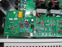
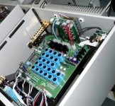
I was looking at the PCBs and I see, if I'm not mistaken, at the speaker output, a circuit with a relay for delayed insertion and, I think, protections for offset voltages.
It seems like a similar circuit to me because, if I'm not mistaken, the UPC 1237 chip is used.
Can we know something more?
Also because, through the usual wholesaler channels, I can no longer find this UPC1237.
Is there something similar as a circuit, but without 1237?
P.S.
instead of the 2n5566 which costs a lot, I use the jfe 2140, very interesting
instead of the 5551 and 5401 singles and then selected, I use FMBM 5551 and 5401
Thanks @Walkalone and @domenico80 for your answers.
I bought the boards from a leer at marktplaats.nl but I'm not really sure If I will build anything with them or will be sold. I had to admit this is a bit complicated for me, although I'd like to try:
So, should I replace U402 with LSK389 or any other?
feedback + connected to BIAS+ and feedback GNG o BIAS- or you mean solder to the solder track feeding the Source pin of all the mosfets??
the board comes with speaker protection circuit based on upc1237 following this schema:
No,
Here is solder pad to feedback the signal into front-end card. Imagining there are 3 points to connect OPS board to FE card: BIAS +; BIAS -; FEEDBACK. Of course including its GND.
// Firstly Use U402 to test, ensure that the circuits operate as nornal.
Here is solder pad to feedback the signal into front-end card. Imagining there are 3 points to connect OPS board to FE card: BIAS +; BIAS -; FEEDBACK. Of course including its GND.
// Firstly Use U402 to test, ensure that the circuits operate as nornal.
Attachments

I really appreciate your help @Walkalone
Both boards has pads for Bias+ Bias - Bias_GND I suppose that interconnection between them would be enough.
The solder pad you pointed me is connected to mosfets source pin.
Both boards has pads for Bias+ Bias - Bias_GND I suppose that interconnection between them would be enough.
The solder pad you pointed me is connected to mosfets source pin.
It looks ok for connections.
But grounding scheme seems complex. If BIAS + and BIAS - go together with its GND, it makes ground loop.
On otherhands, the FEEDBACK must goes with GND due it's inverting input, it also make ground loop.
Complicated grounding may contain hidden ground loops.
But grounding scheme seems complex. If BIAS + and BIAS - go together with its GND, it makes ground loop.
On otherhands, the FEEDBACK must goes with GND due it's inverting input, it also make ground loop.
Complicated grounding may contain hidden ground loops.
Attachments
Thanks for your answer.
Regarding to PSU and GND, and because I do not have the original PSU, I was thinking to do the following for each channel:
OPTION 1:
Regulated (+/-60vdc)+ Unregulated (+/-80 vdc) PSU for the whole system
Mosfets will run unregulated vdc and
driver stage, feedback and pre input at input board will run regulated vdc.
All GND connected to the same point with AC GND connected as well.
OTION 2:
PSU 1: +/- 60vdc unregulated for mosfets.
PSU 2: +/-60vdc regulated for driver stage, feedback and pre input at input board.
Psu1 GND all together and PSU2 GND all together. None of them interconnected and both isolated from the AC input GND. Boards would be isolated from AC GND as well.
Do not connect regulated voltages to drivers, in your boards it's supplied by 4 resistors 10R.
You can use 2 PSUs to supply the power: 1 for power MOSFETs and drivers, 1 for input board. But it must be connected 0V at output of each PSU to create GND. The term ''GND'' is only one, it's reference point of every circuits. Before that point, it is only called ''0V''. From this GND point you can run to OPS board, front end card or speaker return...
See photo below to understand what i say. I do not know GM connected GND wire of feeback or not, or just soldered one end. Because if GND wire connected, it creates ground loop (the loop of ground between input board and output board, you can draw it and see that is a circle).
Years ago i also did GM same as you now, but i do not connect GND end to output board.
Attachments
I really appreciate your help very very much @Walkalone. All of you can see I have not too much skills in amps or PSU design but, since I paid a considerable amount of money for the boards I would like to build the amp.
So, main board for each channel will be feed by 800VA Toroid 2x40VAC so I can feed drivers and mosfets with unregulated +/-57V
The input board VCC_PRE / VEE_PRE can be feed by another PSU 50VA toroid 2x40VAC regulated... or can I connect everything to the same main PSU?
ALL GND together (0 V) unless feedback GND that won't be connected anywhere. Feedback input will be conected to the output speaker in the pad pointed.
If this is all Ok... I think I will start this project.
I would recommend you try by one power to process more easier: unregulared voltages for whole circuits. Upgrade after.
To use lower voltage than standard, need to pay attention at 2 points: cascode voltage for JFET and resistor to reduce power dissipation of CCS transistor (R9). I see in your input board that cascode voltage is calculated as ratio between 33K and 10k = 13V. R9 = 6K2 => both condition is OK.
To use lower voltage than standard, need to pay attention at 2 points: cascode voltage for JFET and resistor to reduce power dissipation of CCS transistor (R9). I see in your input board that cascode voltage is calculated as ratio between 33K and 10k = 13V. R9 = 6K2 => both condition is OK.
Well, let’s pray that this won’t explode in my face 😂
I could go for higher voltage, but my actual PSU boards fits 63VDC caps and that’s the why I should go for 40vac toroids.
Thanks for your support @Walkalone
I could go for higher voltage, but my actual PSU boards fits 63VDC caps and that’s the why I should go for 40vac toroids.
Thanks for your support @Walkalone
Just for an update, the front end board has a common "GND" btw input, feedback, BIAS and A_GND, so no need to make any connection and If using just one PSU al GND will be joined to 0V


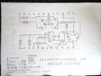
Thank you for the precious images.Hi all,
Finally, the module PCB arrived. Very tiny.
I drew a wiring diagram based on the image of the board you provided.
I apologize for being an amateur, but there are two places where the resistance values are unclear.
Could you please comment on this when you have the time?
Attachments
- Home
- Amplifiers
- Solid State
- Goldmund Wiki and build 2017