Hey.. Mr. Bimo, can u tell more about ur job, detail please..
What job? 😀
He.. I mean sim job 🙂
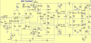
OK, I will explain the schematic as far as my understanding 😀
This amp use 4 stage amplification (according Mr. Self, he count output stage as "stage").
First stage is LTP (Q1 and Q2), it compensated by R8 and C5 to add dominant pole.
Second stage is LTP also (Q3 and Q4).
Third stage is push pull VAS (Q9 and Q11) with Hawksford cascode (Q20 and Q21). To use push pull VAS, the output from Q3 must be invert using Q7 which is cascoded by Q8 (to share the dissipation).
Fourth stage is 3EF.
C6 is lead compensation. Because it does not use Miller compensation, the slew rate is high.
Ok.. iam try to understanding this he.. , iam ever seen this configuration, make 2 stage on input can increase slew rate, but i forget that article say come from. my bad.
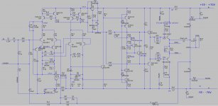
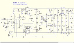
Here's a Survivor I built with a couple of extra tricks.
For one -- it uses an added pole and zero in the 2nd stage to add some extra loop-gain roll-off. Loop gain goes a hair past -180 degrees but not too far into "conditional stability". This allows more in-band feedback and lighter compensation elsewhere.
For two -- it adds a zero in the OPS, well above the ULGF, which cancels some of the excess phase from OPS poles. This allows for a simulated gain margin of 20db. (I borrowed this trick from the NAD 2600 which does the same thing for the same reason. No idea where it originated.)
In my old age, I'm increasingly allowing generous gain and phase margins. 45 degrees and 10db are not enough. 60 degrees and 15db or better are getting there. Is this superstition? Maybe but it can't hurt.
For three -- it uses a speedup cap. I hope that's safe in an EF3. The simulator loves it anyway.
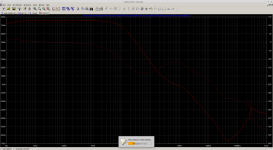
Schematic and loopgain plot attached. The schematic omits the output transistors because they're off the board -- suffice it to say that NDRV and PDRV drive the bases of two pairs of outputs through 4.7 ohm base-stopper resistors. The outputs' emitters return to VOUT. Use your imagination -- the omitted elements are just bog standard.
For one -- it uses an added pole and zero in the 2nd stage to add some extra loop-gain roll-off. Loop gain goes a hair past -180 degrees but not too far into "conditional stability". This allows more in-band feedback and lighter compensation elsewhere.
For two -- it adds a zero in the OPS, well above the ULGF, which cancels some of the excess phase from OPS poles. This allows for a simulated gain margin of 20db. (I borrowed this trick from the NAD 2600 which does the same thing for the same reason. No idea where it originated.)
In my old age, I'm increasingly allowing generous gain and phase margins. 45 degrees and 10db are not enough. 60 degrees and 15db or better are getting there. Is this superstition? Maybe but it can't hurt.
For three -- it uses a speedup cap. I hope that's safe in an EF3. The simulator loves it anyway.
Schematic and loopgain plot attached. The schematic omits the output transistors because they're off the board -- suffice it to say that NDRV and PDRV drive the bases of two pairs of outputs through 4.7 ohm base-stopper resistors. The outputs' emitters return to VOUT. Use your imagination -- the omitted elements are just bog standard.
Attachments
Sure can.
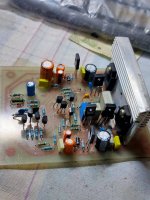
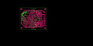
This PCB is a drop-in fit for the Pioneer SA-9500 II chassis which is hosting this build. For the bottom edge connectors I am using Euroblock connectors.
The outputs, base-stopper resistors, ballast resistors, and distributed zobel network live on little daughterboards that bolt up to the heatsink -- hence their absence.
This ".pcb" file is for the open-source pcb program. Not the standard layout tool here but it's what I've been using. I have a script that takes the netlist from LTspice and reformats it into the netlist that pcb expects, so PCB can draw the "rats nest" and check connectivity. Someday I'll post about that.
This layout predates a few circuit elements added after the fact:
So it's a prototype quality layout -- due to be revised.
This PCB is a drop-in fit for the Pioneer SA-9500 II chassis which is hosting this build. For the bottom edge connectors I am using Euroblock connectors.
The outputs, base-stopper resistors, ballast resistors, and distributed zobel network live on little daughterboards that bolt up to the heatsink -- hence their absence.
This ".pcb" file is for the open-source pcb program. Not the standard layout tool here but it's what I've been using. I have a script that takes the netlist from LTspice and reformats it into the netlist that pcb expects, so PCB can draw the "rats nest" and check connectivity. Someday I'll post about that.
This layout predates a few circuit elements added after the fact:
- the 1uF speedup cap
- the 15k "Rmod" resistor which fixes the range on the bias spreader pot to be usable. If you were doing a build from scratch, Rmod isn't needed -- just reduce R42 a bit.
- the 390p and 150R's facing the bases of the drivers. These add a zero to the output stage, well north of ULGF. These aren't strictly needed -- I ran the amp without them for the first couple years -- but it lets us hit 20db of gain margin on the sim.
- D8 and D15 as shown on the layout interfered with the clip that holds the board in place and I had to move them (and grind off some trace to avoid the clip shorting it.) Whoops.
So it's a prototype quality layout -- due to be revised.
Attachments

A couple more thoughts on that layout:
Rtest_pcb allows testing the PCB in isolation with no outputs attached. It's either a jumper (test mode) or open.
Q17 is the bias spreader's temp sensing bipolar. It's a TO-220 with long legs -- soldered to the component side of the board, bent upward 90 degrees and then bolted to a 15 or 20mm standoff which bolts into the heatsink. This is easy to assemble and disassemble and it seems to work well. I'll have to get a pic. There's no connector to come loose and open the bias spreader and fry the outputs, so that's nice!
You can see a number of jumpers, some green and some orange. Notably, the one below R28 carries the output signal back to the negative feedback network. As drawn, it's really too close to the bottom-edge pads where the NPN and PNP output currents meet. If built as drawn, there's risk of introducing halfwave-rectified voltage into the feedback network. So that's a bug. My actual build takes the NFB signal from further away.


Hello jpc2001
greetings at 55 volt dc rails how much base voltages on output transistors
and how much bias voltages over emitter resistances.
warm regards
Andrew
greetings at 55 volt dc rails how much base voltages on output transistors
and how much bias voltages over emitter resistances.
warm regards
Andrew
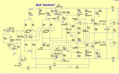
GLA survivor
Hello jpc2001
greetings i have tested the first schematic its sounding very
clear my DC supply rails is +/- 55 volts i need about 150watts
per channel in 8 ohms so i am using 4 pairs 5200/1943
the next 2 schematics i want to try cascode version will it
sonically and stability BETTER than the first schematic PLEASE
i need your advice.Which is better Cascoded or GLASUI H.😕😕😕
warm regards
Andrew
Attachments

Veysel, I assume you're talking about the schematic in post 112 where R27 is a 39 ohm part.
Cordell addresses this in his book. IIRC a bias spreader without this resistor isn't a perfect "voltage source". It has some finite impedance. If the current through the bias spreader fluctuates, the B-E voltage fluctuates slightly and so does the whole bias voltage. The resistor compensates for that. Cordell recommended values near 15 ohms (for EF2?) and this one is higher (because it's EF3?)
Cordell addresses this in his book. IIRC a bias spreader without this resistor isn't a perfect "voltage source". It has some finite impedance. If the current through the bias spreader fluctuates, the B-E voltage fluctuates slightly and so does the whole bias voltage. The resistor compensates for that. Cordell recommended values near 15 ohms (for EF2?) and this one is higher (because it's EF3?)
- Home
- Amplifiers
- Solid State
- GLA (good little amp) "survivor"