Because someone asked 🙂
Use of the final stage only as a unity gain buffer.
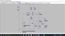
Same supply voltage and seems capable of delivering the 2 volts rms (CD standard output) required into 600 ohms. In fact it is pretty good right up to 2.25 vrms on a 6.8 volt supply which is quite remarkable really. Bias resistors will need setting experimentally and so will the coupling caps to suit your requirements. The input impedance will be pretty low and so a 47uF for the input may be as low as you can go.
Much depends on the germanium device used and how much gain it has and so consequently how low in value the bias network will have to be.
Use of the final stage only as a unity gain buffer.
Same supply voltage and seems capable of delivering the 2 volts rms (CD standard output) required into 600 ohms. In fact it is pretty good right up to 2.25 vrms on a 6.8 volt supply which is quite remarkable really. Bias resistors will need setting experimentally and so will the coupling caps to suit your requirements. The input impedance will be pretty low and so a 47uF for the input may be as low as you can go.
Much depends on the germanium device used and how much gain it has and so consequently how low in value the bias network will have to be.
Attachments


...input impedance will be pretty low...Much depends on the germanium device used and how much gain it has and so consequently how low in value the bias network will have to be.
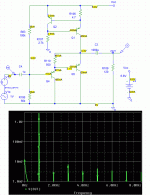
Which can be designed-away at the cost of one more transistor. Darlington is certainly in the family. Zin is 30k all over the audio band. Bandwidth as shown is 5cps up (I don't trust my model at RF, but an emitter follower will be OK past 20KC).
Random changes:
I drew it plus-up so I did not have to think on my head. It can work either way of course. Plus-up *may* be convenient to share power with other loads.
The 40mA(?) is over 100mW which seems hot for many GE devices. And 3V/40mA seems good to under 100 Ohms, better than the 600r load shown promises. I split-difference at 30mA and 120r.
THD at 120 load and 2.7V peak is 0.36% and clipped; all harmonics showing. At 2.4V peak the idiot figures 0.2% and a nice fall of high harmonics.
Code:
*AC127 PNP Germanium Transistor Spice Model
*alternate: NF=0.5 Is=10EE-8
.MODEL AC127_XP PNP (
IS=10u
NF=1
NR=1
ISE=0.5u
ISC=1u
NC=1.5
NE=1.5
BF=90
BR=5
VAF=40
VAR=40
RB=100
Rc=10
EG=0.67
CJC=10p
CJE=8p
VJC=0.25
VJE=0.25 )
*$
Attachments
Last edited:
I use a complementary feedback pair in mine, with both Ge and Si. The Ge is the input transistor and the Si is the output transistor running at 100mA, with a single Si constant current source for bias. The Ge transistor dominates the sonics as the silicon BD139 is within its feedback loop. I’ve not measured the distortion yet but it should be lower than a darlington emitter follower.
Why use germanium? Because although they are outperformed by silicon transistors in many ways, I enjoy their sonics. Yes, they are acting as tone enhancers. Too many of them in the signal path can be excessive though.
All too often a circuit has been designed with the lowest distortion possible, and I’ve designed some very low distortion circuits over the years. But haven’t these circuits lost sight of the sonics as entertainment? Hifi is for entertainment after all, isn’t it?
All too often a circuit has been designed with the lowest distortion possible, and I’ve designed some very low distortion circuits over the years. But haven’t these circuits lost sight of the sonics as entertainment? Hifi is for entertainment after all, isn’t it?
USSR p-n-p and n-p-n germanuim transistors
.
.
.
.
.
.
.
.
Code:
* ГТ308Б
.model GT308B pnp
+bf=800
+br=0.3e+000
+eg=0.72e+000
+cje=20e-012
+cjc=15e-012
+tf=1e-009
+tr=0.4e-006
+xcjc=0.4e+000
+is=100e-009
+ikf=45e-003
+vaf=30
+mje=0.5e+000
+mjc=0.5e+000
+rc=20
+rb=80
+rbm=10
+irb=1e-003
+ise=25e-009
+ne=1.5e+000
+isc=0.7e-006
+nc=1.4e+000
+mfg=USSR
Code:
* ГТ322А
.model GT322A pnp
+bf=100
+br=0.3e+000
+eg=0.72e+000
+cje=10e-012
+cjc=4e-012
+tf=1e-009
+tr=0.4e-006
+xcjc=0.3e+000
+is=50e-009
+ikf=20e-006
+vaf=30
+mje=0.5e+000
+mjc=0.5e+000
+rc=10
+rb=40
+ise=10e-009
+ne=1.5e+000
+isc=0.5e-006
+nc=1.4e+000
+mfg=USSR
Code:
*ГТ310Б © Сухов, 2017
.MODEL GT310B PNP
+BF=200
+BR=100M
+CJC=5P
+CJE=2P
+IKF=1
+IKR=1
+IS=10F
+ISC=1P
+ISE=1P
+ITF=10M
+MJC=500M
+MJE=500M
+NE=2
+RC=500M
+RE=500M
+TF=1N
+TR=10N
+VAF=100
+VTF=10
+XTF=500M
Code:
* ГТ311А
.model GT311A NPN
+IS=14e-012
+TF=10.7e-009
+TR=0
+Cje=10e-012
+Cjc=7.5e-012
+VJC=0.6e+000
+BF=71.4e+000
+BR=1.3e+000
+RB=100
Code:
* ГТ404Г
.MODEL GT404G NPN
+BF=160
+BR=9.4
+CJC=2.86n
+CJE=2.08n
+EG=0.67
+IKF=2.5
+IKR=200m
+IS=28u
+ISC=800n
+ISE=1.55u
+ITF=11.194m
+MJC=3.5
+MJE=4.05
+NE=2
+NF=1.09
+RB=5
+RC=100m
+RE=440m
+TF=113n
+TR=448.17n
+VAF=35
+VTF=10
+XTF=500m
Code:
* ГТ402Г
.MODEL GT402G PNP
+BF=200
+BR=9.5
+CJC=580p
+CJE=400p
+EG=0.67
+IKF=3.5
+IKR=500m
+IS=4.9u
+ISC=300n
+ISE=180n
+ITF=40.9u
+MJC=3.9
+MJE=5.7
+NE=1.9
+NF=1.1
+RC=200m
+RE=400m
+TF=75.56n
+TR=96.58n
+VAF=18.3
+VJC=850m
+VJE=850m
+VTF=10
+XTF=1.79
Last edited:
Which can be designed-away at the cost of one more transistor. Darlington is certainly in the family. Zin is 30k all over the audio band. Bandwidth as shown is 5cps up (I don't trust my model at RF, but an emitter follower will be OK past 20KC).
Random changes:
I drew it plus-up so I did not have to think on my head. It can work either way of course. Plus-up *may* be convenient to share power with other loads.
The 40mA(?) is over 100mW which seems hot for many GE devices. And 3V/40mA seems good to under 100 Ohms, better than the 600r load shown promises. I split-difference at 30mA and 120r.
THD at 120 load and 2.7V peak is 0.36% and clipped; all harmonics showing. At 2.4V peak the idiot figures 0.2% and a nice fall of high harmonics.
Plus up 😀 I like that 🙂
Actually I think you will find your configuration gives a bit better high frequency ripple rejection (as long as you leave ground where you have it) because the current sink/source is now fed from the rail and is not in the earthy side. For a battery headphone amp it doesn't matter of course.
USSR p-n-p and n-p-n germanuim transistors
.
Thanks 🙂 It is always useful to have a resource of such things.
P27B (Russian П27Б)
Low noise p-n-p germanium tranistor.
Uce, max = 5V
.
.
.
.
.
.
.
.
HF and UHF transistor.
.
.
Low noise p-n-p germanium tranistor.
Uce, max = 5V
.
Code:
* П27Б
.MODEL P27B PNP
+BF=135e+000
+BR=6
+EG=0.68e+000
+CJC=200e-012
+CJE=200e-012
+FC=500e-003
+IKF=150e-003
+IKR=100e-003
+IS=780e-009
+ISC=750e-009
+ISE=295e-009
+ITF=9.95e-003
+MJC=825e-003
+MJE=500e-003
+RB=200
+NC=1.335e+000
+NE=1.67e+000
+NF=850e-003
+RC=5
+RE=4
+TF=47.6e-009
+TR=560e-009
+VAF=17e+000
+VJC=700e-003
+VJE=500e-003
+VTF=10
+XTF=500e-003
Code:
.model AC128 PNP
+Bf=70
+Vje=0.2
+Is=1.41f
+Xti=3
+Eg=1.11
+Ne=1.5
+Ise=0
+Ikf=80m
+Xtb=1.5
+Br=4.977
+Nc=2
+Isc=0
+Ikr=0
+Rc=2.5
+Cjc=9.728p
+Mjc=0.5776
+Vjc=0.2
+Fc=0.5
+Cje=8.063p
+Mje=0.3677
+Tr=33.42n
+Tf=179.3p
+Itf=0.4
+Vtf=4
+Xtf=6
+Rb=10
Code:
* МП39Б
.model MP39B pnp
+bf=140
+br=3
+eg=0.72
+cje=30p
+cjc=90p
+tf=0.2u
+tr=1.u
+is=3u
+ikf=50m
+vaf=15
+mje=0.5
+mjc=0.5
+rb=150
+rbm=50
+irb=0.1m
+ise=.3u
+ne=1.28
+isc=0.6u
+nc=1.28
+mfg=USSR
Code:
* МП41
.model MP41 pnp
+bf=140
+br=4
+eg=0.72
+cje=30p
+cjc=90p
+tf=0.1u
+tr=1.u
+is=3u
+ikf=50m
+vaf=15
+mje=0.5
+mjc=0.5
+rb=150
+rbm=50
+irb=0.1m
+ise=.3u
+ne=1.28
+isc=0.6u
+nc=1.28
+mfg=USSR
Code:
* МП37
.model MP37 npn
+bf=140
+br=4
+eg=0.72
+cje=30p
+cjc=90p
+tf=0.1u
+tr=1.u
+is=3u
+ikf=50m
+vaf=15
+mje=0.5
+mjc=0.5
+rb=150
+rbm=50
+irb=0.1m
+ise=.3u
+ne=1.28
+isc=.6u
+nc=1.28
+mfg=USSR
Code:
* МП35
.model MP35 npn
+bf=140
+br=4
+eg=0.72
+cje=50p
+cjc=90p
+tf=0.2u
+tr=2.u
+is=3u
+ikf=50m
+vaf=15
+mje=0.5
+mjc=0.5
+rb=150
+rbm=50
+irb=0.1m
+ise=0.3u
+ne=1.28
+isc=0.6u
+nc=1.28
+mfg=USSR
Code:
* МП25А
.model MP25A pnp
+bf=140
+br=3
+eg=0.72
+cje=30p
+cjc=90p
+tf=0.4u
+tr=4u
+is=3u
+ikf=40m
+vaf=30
+mje=0.5
+mjc=0.5
+rb=120
+rbm=40
+irb=0.1m
+ise=.3u
+ne=1.28
+isc=.6u
+nc=1.28
+mfg=USSRHF and UHF transistor.
.
Code:
* П416Б
.model P416B pnp
+bf=800
+br=.3
+eg=0.72
+cje=20p
+cjc=15p
+tf=1n
+tr=.4u
+xcjc=0.5
+is=100n
+ikf=45m
+vaf=30
+mje=0.5
+mjc=0.5
+rc=20
+rb=80
+rbm=10
+irb=1m
+ise=25n
+ne=1.5
+isc=.7u
+nc=1.4
+mfg=USSR
Last edited:
Why not germanium ?
It's a fun project that has turned out surprisingly well 🙂
I've been a member of the Ge cult for many years.
Did a open loop one transistor door-knob 2n442 to36 power amp years ago.
The output was only a few watts but it sounded metaphysical.
Speakers were minimus7.
Bandwidth was limited by the device's hole speed. Maybe that is the secret.
Congrats on using for headphone.
Mooly I built a breadboard version of your design using mp26b and an mp10b transistor. It works pretty well and sounds good but I suspect my output stage needs adjusted. Q3 is drawing more current than Q4. What voltage should the emitter of Q3 be? Mine is about 4.5v now with a 7v supply. The collector of Q6 is close to 1/2 of the supply voltage as you mentioned. Thanks.
Emitter of Q3 should be around half the supply voltage so as to give symmetrical clipping, so around -3.5 volts with a -7 volt supply.
If the Collector of Q6 is correct then the emitter of Q3 should essentially follow it in voltage as it is just an emitter follower.
So that actually suggests a problem with Q3. The base/emitter volts (measured across the junction) should be pretty low at around -150 millivolts with the base the more negative. There should be virtually no voltage across the 27 ohm (R9)
Maybe that particular device just isn't suitable and is going into some kind of thermal runaway and low gain state (germanium devices are prone to this at far far lower temperatures than silicon).
A picture is worth 1000 words so here are my measured voltages. The negative supply threw me off so disregard my previous numbers. Q6 isn't quite half the supply but close enough I gather. The base/emitter voltage of Q3 is reading -0.3v. The voltage across R9 is -31mv.
Attachments

Lets go back to basics...
The current in Q3 and Q4 should be essentially identical. This is the total current flowing in R10, the 3.3 ohm.
That resistor can be tweaked to give more or less bias current, the effect of that is to allow higher current delivery into lower impedance loads.
The voltage on Q3 emitter sets whether the amp clips symmetrically or not and should be around half the supply voltage. Ideally use a scope and a suitable load resistor to get the max undistorted voltage swing across the load.
You should be able to set that via tweaking R13, the 33k.
The first stage has no effect on the output stage biasing but the emitter of Q1 should also be around half the supply voltage. That can be tweaked via R4
The nature of germanium devices in combination with a low supply voltage and relatively high value resistor networks for setting the DC conditions mean that the circuit can be a bit critical on devices used unless you do tweak values. With silicon the specs are more consistent and gain much higher and so repeatability is better.
Great explanation, thanks for taking the time to help me understand. R13 had to be decreased to 28k.
Recently i got an interest in germanium trz just because of a friend of mine and also because i got a signifiant number of ac180, ac181, ac 187 and ac188 and i'd like having some close ltspice models for them if possible just to play a bit outside the well known germanium territory.Could anybody help me with that?
I know there's some equipment able to make a spice model out of tube measurements done automatically .Is there anything simillar for transistors?I haven't found any really good models. All I have are these put together from what I've found on the forum.
I don't know is the honest answer. Making models is something I have never got involved with.
The best place to ask would probably be in the LT thread (click my signature line). There is a lot of knowledge there.
The best place to ask would probably be in the LT thread (click my signature line). There is a lot of knowledge there.
I knew your thread and i thought you must be the most competent voice about it , it's just that I didn't want to pollute that thread with germanium "crap"... as some guys tell very firmely germanium is all about when anything about germanium trz is up so i wanted to keep it local.
I think that germanium transistors deserve their own Section in the Forum because , apparently there's a real following same as with the tube following, just maybe a bit shy, but your topic on Germanium Headphones amplifiers might become a Forum section by itself, but you're a moderator and hijaking your thread might not be the wisest thing I could do 🙂 . Yet it seemed to me to be a dormant topic that has a Dragon life of itself due to that VBE refferenced CCS you used which was the first to raise some questions in my mind about germanium junction compensation.
Having a transistor open at 0.1v BE seems to be a big deal to me and some other past experiences of mine pushed me towards a new take on on amps that need some sort of soft compression here and there .Besides all that it's your topic along with the existence of a friend's amp that has a germanium superdiode to regulate the junction tempco of some old germanium transistors that gave me the momentum to start simulating around a diamond buffer which technically is solving the temp compensation in the first place, but i thought of containing the germanium thermal runaway by enclosing a germanium diamond buffer made by q1, q2, q3, q4 inside another silicon trz based diamond buffer made out of q6, q7, q9, q10 aided by R8 and r9 as NTC.
Until now all my simulations were made around silicon transistors so i just assumed that keeping q2 and q3 also silicon trz and q1 q4 germanium i'd only have to use r8 and r9 as NTC and raised R1 and R2 to equal for 0.55v-0.1v /Ie would allow for paralleling many germanium trz cascoded or bootstrapped by single higher power silicon Q9 and Q10 if i want high power amps made with low VCE trz like ac187/ac188 or ac180/181 which happens that i have a lot of them.As germanium trz exhibit leakage and poor frequency response , limiting the inrush current and having them cascoded or even bootstrapped by silicon trz looks like a better use for them.
Besides i like having all related information in one place, easy to find , more than creating new topics on the same theme.For the moment we don't have a Germanium corner...
Attachments

Last edited:
- Home
- Amplifiers
- Headphone Systems
- GERMANIUM Single ended Class A Headphone Amp.