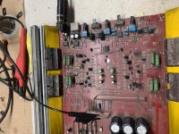
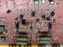
Need some help folks, been several years since I worked on a class AB. I got what seems to be an SPL 2 channel amplifier in, single layer board. It had burnt PS FETs and output transistors. After much tinkering and parts replaced I got the amplifier working, however one side is way louder than the other. With 920mV being inputted from the SG. I have 17.5 vrms on the left channel at the output and 4.25 vrms on the right, both clean sine waves. If I increase the input signal the left channel begins to clip way before the second channel. I’ve done some probing in the driver circuits. Both circuits have approximately 2.8v rms entering the differential pairs but after this it goes haywire.
Any help as to what I’m overlooking/forgotten?
Any help as to what I’m overlooking/forgotten?
Attachments
The gain of the power amplifier section is determined by the feedback to the inverting side of the differential pair. The following amp diagram may or may not be similar to yours but it's good enough to show you where you need to look.
The gain is determined by Cx54, Rx70 and Rx65.
The gain is determined by Cx54, Rx70 and Rx65.
Attachments
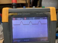
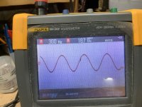
I checked the feedback components as suggested, all three are within tolerance, I replaced the cap with a new as a precaution. The amp still has a higher gain on the left channel. I checked waveforms vs the right channel and the only thing different I’m seeing are the waveforms on the emitter (first pic) collector (second pic). Seems to be a half regulated wave. I replaced Q216 But it didn’t go away. The amp passes clean wave though (pic three). I think Q216 is associated with the protection circuitry, but its being fed from the output. Any other suggestions to get the gains matched/close?
Attachments
Q216 shouldn't affect the gain of the channel.
The collector should only have clean DC. The base and emitter should have the output signal.
Confirm that the emitter resistors are within tolerance.
The collector should only have clean DC. The base and emitter should have the output signal.
Confirm that the emitter resistors are within tolerance.
Although it won't affect the gain, it appears that the transistors is installed incorrectly or you have the wrong pin configuration.
Are you absolutely sure that the input to the two channels at the base of the differential pair is identical?
Are you absolutely sure that the input to the two channels at the base of the differential pair is identical?
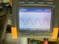
The first pic is the base of q202 and the second is the base of 204. The signals are more or less the same here.
The signal moves onto q205 and 206, At the bases I get rail voltages, there are ceramic caps across the base of q205 and q208.
On the cap (side connected to base of q208) I get a signal of 19.2v rms on the other side of the cap (side connected to collector of q205) I get straight rail voltage.
The same for q206 and q209, but negative rail voltage.
This has me stumped. The pcb is mirrored I looked again at the components and the orientation and connections.
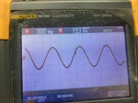
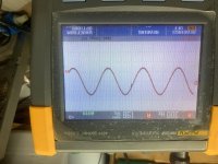
I scoped the right side and the the signals are the same but at a lower amplitude (4.26v rms) with the same 700mV signal being inputted on both channels.
The signal moves onto q205 and 206, At the bases I get rail voltages, there are ceramic caps across the base of q205 and q208.
On the cap (side connected to base of q208) I get a signal of 19.2v rms on the other side of the cap (side connected to collector of q205) I get straight rail voltage.
The same for q206 and q209, but negative rail voltage.
This has me stumped. The pcb is mirrored I looked again at the components and the orientation and connections.
I scoped the right side and the the signals are the same but at a lower amplitude (4.26v rms) with the same 700mV signal being inputted on both channels.
Attachments
Last edited:
Are the values of the components in the two channels identical?
Do you see the same signal on all of the terminals of those components, comparing the two channels?
Do you see the same signal on all of the terminals of those components, comparing the two channels?
Yes sir. After I got the amp up and started troubleshooting the gain problem, I even swapped one component at a time from the right channel to the left.
Before you posted the schematic I checked the value of each component on the left vs the right ( this was before swapping). After I got the schematic I did some random checks on component values and they checked ok.
From the schematic side though, and looking on the board, the pcb doesn’t have q107 and 207, but as you said my amp is prolly a different model.
Does the signal on the input side of the differential amp match, exactly, the input to the feedback side of the differential amp, on both channels?
That's close enough.
Have you tried increasing the value of the feedback resistor Rx70 to see if you could get the low side to match?
Could you have any electrical leakage on the board (electrolyte or fixative)?
Have you tried increasing the value of the feedback resistor Rx70 to see if you could get the low side to match?
Could you have any electrical leakage on the board (electrolyte or fixative)?
No,I haven’t messed around with different values. But I’ll do so now, seemingly it checks good thus far.
I soldering in a 10k pot in place of the feedback resistor, however the amplitude came down with decreasing the resistance. I matched both sides and the final resistor was a 1k I soldered in.
Amp was benched tested for just over an hour on the dummy load, everything worked ok.
Thanks for the assistance.
Amp was benched tested for just over an hour on the dummy load, everything worked ok.
Thanks for the assistance.
- Home
- General Interest
- Car Audio
- Generic AB amplifiers