I've been watching this thread with interest - it seems to be a nice 'GC ' variant (esp. vs the Bridgeclone).
As gainclonin is where my heart currently lies (I know there are different things out there too), have you tried this in inverting mode, with a T network on the feedback loop..???
This could be very interesting, as it will help isolate the driver stage from the speaker variation in the feedback loop.
Very good things have been heard with the T network mod in inverting mode, and this could be a valuable route to persue..
So, some thuoghts, and back to lurk mode..
Owen
Ok, now I also forgot to add this....
Transformers
These guys have a small mu-metal audio TX that is flat at 1mW from 20Hz to 35KHz, and is a centre tapped for balanced to unbalanced and vice versa.. downside is they are designed for PCB usuage 🙄
Have fun
Owen
Transformers
These guys have a small mu-metal audio TX that is flat at 1mW from 20Hz to 35KHz, and is a centre tapped for balanced to unbalanced and vice versa.. downside is they are designed for PCB usuage 🙄
Have fun
Owen
owen said:As gainclonin is where my heart currently lies (I know there are different things out there too), have you tried this in inverting mode, with a T network on the feedback loop..???
This could be very interesting, as it will help isolate the driver stage from the speaker variation in the feedback loop.
I assume you are talking about resistively connecting the
negative input to ground to "throw away" some open loop
gain, and thus reduce the amount of feedback. I addressed
this in an earlier thread "7 easy pieces", and I'm certain others
have thought of it as well.
The value is not that of isolation, but reduction of feedback,
which increases the phase margin of chip amps, making them
more frequency stable and generally making them sound better.
😎
I just finished doing some reading over in the chipamp forum to figure out exactly what Owen was meaning. This T-network is referring to using a voltage divider in the chips feedback loop. The purpose being to allow the signal to be input to the chip through the negative input with the positive input grounded, while maintaining a high input impedance to the chip without having to resort to very high feedback resistor values that increase circuit noise.
Well, can this circuit be modified to operate the chips in an inverted configuration? Certainly! Even better, I don't believe that the T-network would be required. As I mentioned above, the purpose of the T-network is to allow a higher value resistor to be used at the negative input to the chip to increase the input impedance without requiring a large value resistor to be used in the feedback position. With the bipolar transistors in the differential pair front end of the XGC there is current drive aplenty, so there isn’t a need to keep the input impedance to the chips high, thus eliminating the need for the T-network.
Will there be a benefit to implementing the chips in an inverted configuration? I haven’t the slightest clue! I keep seeing references that say that it is superior, and even hints that John Lindsay Hood proved why, but I haven’t found the exact explanation yet, so I can’t really comment.
In the meantime Owen, it should be pretty simple to implement your idea, so give it a try at let us know how it turns out!
As to eliminating the effect of the speaker variation on the driver stage, I think that in this topology, the interaction between the speaker and the input differential is actually one of its benefits, one that give this circuit such great control over the speakers. With the combined effect of the balanced topology and the supersymetric feedback, the interaction between the speaker variation and the input differential is mirrored identically on each side of the balanced circuit effectively negating it through cancellation.
I hope I got this last bit right! If not, Nelson or some of the other gurus can jump in and correct me.
Cheers, Terry
the advantage as I understand it is this:
with an inverting design the + i/p is held at 0V. When a signal is introduced the o/p moves to keep the - i/p the same as the + i/p
this means they both stay more or less at zero
If the i/p's move with the signal, as they do with non inverting configuration, it cause some kind of distortion.
So, according to theory, - if all other things are equal, inverted configuration sounds best
with T network the F/B impedance is able to be kept low so, as far as I can understand it, all other things are equal.
hope this helps
mike
As op-amps go, and generically speaking, inverting topology gives lower THD.
Form the LM4780 datasheet:
"The inverting amplifier can have better
THD+N performance and eliminates the need for a large
capacitor (Ci) reducing cost and space requirements."
The advantage is also that you can very easily control (null) DC-offset with some resistance (with a multi-turn trimmer or a fixed resistor) from NI to ground.
No caps needed, as in the non-inverted topology.
To avoid the Ci cap on non-inverting topology you must match impedances.
To do that, if you don't use an input buffer or gainstage, you will end with a low input impedance OR a manageable value but a high value resistor on the feedback.
The inverting t-network allows you to use low value resistors for feedback and a high(er) input impedance.
Also, as Owen said, it gives a path to ground and reduces the effect of the back emf from the speaker being fed back to the input of the amp.
I still get the biggest bang out of throwing away some feedback.
😎
feedback, get thee behind me!
😎
feedback, get thee behind me!
I still feel pretty smug about pulling the line stage together with a whisker over 7dB of NFB. Fooey on people who don't think it's stereo until it's got 50dB feedback.
There's not really anything to keep me from running it with 0dB, and I may yet build a slightly different version that way for my own use.
Grey
There's not really anything to keep me from running it with 0dB, and I may yet build a slightly different version that way for my own use.
Grey
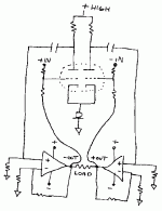
Ok, not sure if this really ought to go here, but it is on topic (a SuperSymmetric GC), but with a triode twist...
So we have a fet based input long tailed pair in the X - that I'd like to replace with triodes (6922), using the same current sink (mosfet).
So, considerations, guidelines, how to calculate the 'supersymmetric' feedback path etc please (remember I'm no EE.. 😀 ) from the anode (drain) to the grid.
I am also a little confused wrt the gain of the chips themselves, as the 'traditional' feedback loop is alot extended...
As the 6922 is a 'low voltage' valve, I will be envisioning a B+ (if you can call it that) of around 50+ volts (ideally a voltage drop of <10 volts or so on the CCS, which should be plenty)
So, some help with some calcs please
 maths
maths
Have fun
Owen
So we have a fet based input long tailed pair in the X - that I'd like to replace with triodes (6922), using the same current sink (mosfet).
So, considerations, guidelines, how to calculate the 'supersymmetric' feedback path etc please (remember I'm no EE.. 😀 ) from the anode (drain) to the grid.
I am also a little confused wrt the gain of the chips themselves, as the 'traditional' feedback loop is alot extended...
As the 6922 is a 'low voltage' valve, I will be envisioning a B+ (if you can call it that) of around 50+ volts (ideally a voltage drop of <10 volts or so on the CCS, which should be plenty)
So, some help with some calcs please
maths Have fun
Owen
owen said:So we have a fet based input long tailed pair in the X - that I'd like to replace with triodes (6922), using the same current sink (mosfet).
That same thought had crossed my mind...
dave
Well, you treat it just like it was some N channel JFETs
(no problem inverting the whole circuit if you were using
P channel JFETs) and provide some seriously high voltages.
Resistors going to the positive rail off the Plates provide the
voltage to drive the rest of the gain stage, most likely through
capacitors. The grids can be operated at ground potential,
and the current source for two connected cathodes needs to
hold the voltage that will represent the Grid-Cathode voltage.
If you take the signal off the plate and just use it to drive
chip amps as followers, or with limited gain, it will work fine
(I think) You might want to take steps to ensure that the
chip inputs aren't overdriven on turn-on.
😎
Attachments
Hi, metalman
I got 4 x LM3875.
I consider to build the same as yours.
Which one is your latest circuit as built?
Thks.
I got 4 x LM3875.
I consider to build the same as yours.
Which one is your latest circuit as built?
Thks.
Hi metalman-
In line with the last post, is your latest circuit good for the LM3875 AND 86 chips?
Does it matter which model chip is used other than the respective pinout?
In line with the last post, is your latest circuit good for the LM3875 AND 86 chips?
Does it matter which model chip is used other than the respective pinout?
jh6you,
The schematic in post #240 is the latest version.
rabstg,
The LM3886 will work fine in this circuit, and might in fact perform better, as it has a lower open loop gain than the LM3875 that should improve overall stability. It will also provide more current ouput into lower impedance speakers. I haven't looked at the pinout configuration, so do check that. I originally chose the LM3875 because A) I wanted to compare performance against an LM3875 standard GC, and B) my speakers have a 6ohm minimum impedance, so I didn't need the extra current drive and the LM3875 gave me a higher max power for my speakers.
Cheers, Terry
The big caps are WIMA MKP 1uF, 27,5mm pitch. I also made a footprint for a less expensive alternative.
//Vit
//Vit
metalman said:The LM3886 will work fine in this circuit, and might in fact perform better...
Everything I've seen points toward this being a more audiophile
grade chip, but I haven't had a chance to refine any designs
using it - too busy with single transistor amplifiers, you know...
😎
vit: you're not putting any larger caps at the chip? I'm not sure how well that'll work (but, that merely means I really have no idea how well it would work.)
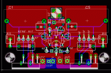
Ironically (or not) I hopped in here today to get an opinion on a PCB. 🙂 Also, revised (corrected really) schematic. 4.25x2.55 inch (~108x65mm) using LM4780's.
Ironically (or not) I hopped in here today to get an opinion on a PCB. 🙂 Also, revised (corrected really) schematic. 4.25x2.55 inch (~108x65mm) using LM4780's.
An externally hosted image should be here but it was not working when we last tested it.
An externally hosted image should be here but it was not working when we last tested it.
vit said:Hi guys. I plan to build xgc as soon as possible. Please comment my pcb. Each channel measures 50x80mm.
cheers // Vit
Maybe it's wise to put Q1 and Q2 close together, to bond them thermally.
Also, I would provide space for caps close to the supply pins. Just look for Carlos FM's suggestions about PSU for chip amps 🙂
- Home
- Amplifiers
- Pass Labs
- GC SuperSymmetry