DS1802 Volume Knob
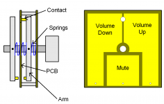
So here is my proposed design for a volume knob for the DS1802. First a basic description of the function. Turn left and right controls volume up and down, the contact pin is kept in contact with the PCB by means of springs. Pulling the knob outward causes the contact at the back to make contact with the PCB (compressing the rear springs) turn left or right to adjust balance. Finally pushing the knob inward while in it's "rest" position allows the upper contact to pass through the hole in the top of the PCB allowing the bottom contact to touch the mute pad. The contact pins are kept at the ground level of the DS1802, the pads on the PCB are connected to the appropriate pins of the DS1802. This may be hard to conceptualize which is why I thought a 3D model would help. Perhaps when I get some more time to actually build it I will post some photos.
The parts should be fairly obvious from the attached picture. Basically two arms (aluminum square rod or similar) are attached to a cricular shaft. A pair of PCB's surround one arm with a pair of springs that keep the main contact touching the volume PCB. The springs should be bent at the tips and inserted into holes in the PCB and the arm which will return the arm to it's rest position when released. Pulling the knob out or pressing it in compresses at least one spring which when released will return the knob to volume mode.
Anyway, take a look at the picture it should be more obvious from that.
Attachments
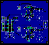
OK So here is the nearly final layout that I'll be using for this preamp. Notice in the picture that I ditched the DIL8 packages for the BUF634 and went for the TO220's. Because this chip is going to run HOT it will need heatsinking...you just can't do that well enough with a DIL package. I also replaced the capacitor in the OPA637 feedback loop with a resistor. This is optional but could be used if there are stability issues. I also added some onboard connectors. I finished my other project for the wife this weekend so I should have some time to etch this design...may need to find some capacitors though....also may be short a few precision resistors.
For those interested in using the DIL8 I will modify the board design that I already had and add a resistor between the V- rail and the BW pin, this should keep things a bit cooler.
So here it is. 😀
For those interested in using the DIL8 I will modify the board design that I already had and add a resistor between the V- rail and the BW pin, this should keep things a bit cooler.
So here it is. 😀
Attachments
Member
Joined 2002
RIGHT ONNNN!!! looks good. When you going to do board's? Are you going to do a test board build one then let us know ?
jleaman said:RIGHT ONNNN!!! looks good. When you going to do board's? Are you going to do a test board build one then let us know ?
Glad you like it...I am definately going to test it first, currently I have no plans to have boards made (I'm etching my own) but if there is enough interest I could possibly be swayed. I'll likely etch 2 this week and send you one in the mail...never hurts to have a second opinion. I'll work on getting the parts values on the boards then post the eagle files too....as long as the wife doesn't find more work for me to do

Member
Joined 2002
Gcollier said:
Glad you like it...I am definately going to test it first, currently I have no plans to have boards made (I'm etching my own) but if there is enough interest I could possibly be swayed. I'll likely etch 2 this week and send you one in the mail...never hurts to have a second opinion. I'll work on getting the parts values on the boards then post the eagle files too....as long as the wife doesn't find more work for me to do
You Got Mail. Reply : O )
To deal with my smd ds's, I can either edit your Eagle files or make a smd-dip adaptor. Maybe I'll take the second route - should be easy enough. I'll just get the DIPs for the next tie around.
I also already ordered samples of the DIP buffers (can you say "jump the gun"?). Maybe I should edit the Eagle files...
Waiting for testing this time. 😉
Keep us up to date...
I also already ordered samples of the DIP buffers (can you say "jump the gun"?). Maybe I should edit the Eagle files...
Waiting for testing this time. 😉
Keep us up to date...
WorkingAtHome said:To deal with my smd ds's, I can either edit your Eagle files or make a smd-dip adaptor. Maybe I'll take the second route - should be easy enough. I'll just get the DIPs for the next tie around.
I also already ordered samples of the DIP buffers (can you say "jump the gun"?). Maybe I should edit the Eagle files...
Waiting for testing this time. 😉
Keep us up to date...
It would likely be easier to buy the DIP version of the DS1802 😉
But...I have attached a ZIP that contains eagle BRD files for both versions of this preamp. I am also going to put together another power supply for this project, it will not be anything fancy though, just a standard regulated supply.
😀
Attachments
Hi Guys
I was just looking at your board design and it looks good and symetrical but some of your gnd current paths look a little long.
The bottom bypass caps are enclosed by the +- rails and the gnd path has to travel in a big circle all the way around the chips. This may or may not have detrimental effects but I would think shorter gnd paths would make for a more sound design.(NPI)
I remember reading somewhere about keeping in mind the current paths when designing boards.
I've been doing single sided boards myself and on one I have used vias for the power so as to maintain the gnd plane.(bigc)
Just my 2 cents worth. Not meaning to start great debate.
Hugh 🙂
I see I was to slow to post .
The changes you've made look much better with the two power connections.
Sorry bout that.
Hugh
The changes you've made look much better with the two power connections.
Sorry bout that.
Hugh
Hugh M said:I see I was to slow to post .
The changes you've made look much better with the two power connections.
Sorry bout that.
Hugh
Yup that is the reason I added the 2 power connectors, I don't like long ground paths either. 😀 But it is always nice to have helpful suggestions!
Thanks!
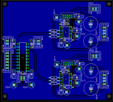
Heres my version of the line stage board. Lots of things could be better but I etched it and it sounds great. I made a new package for the TO-220 5pin cause the spacing on the inline was to close in my test print. I also put the ps on board. Uses dual traffos as I had them lying around from old sat recievers. At the last minute I also decided to put all the 100n bypass caps on the bottom of the board off the component pins.
Hugh
Hugh
Attachments

Member
Joined 2002

jleaman said:Here hows this i'm not done the top one just the bottom one.
Well that layout might look better but I assure you it won't sound better 😉 You've moved the supply decoupling caps too far from the supply pins to be doing any good at all. 😱
Look at what Carlos was saying earlier in this thread, that was my reason for changing the initial DIP design I had. After some more reading I found that this is necessary for high speed opamps. If you want the output close to the pins then use a U shaped heatsink (like my custom ones on my LM338 regulator posted earlier) and put the connector in the U.
I may etch these tonight if I get a chance..I'll see what I have for parts too...maybe by Friday I'll have some results
😀
That looks much better. If I may make a couple of suggestions
1. Move the o/p connector to the top or just to the right of the buf634 and leave clearance for the heatsink.
2. Turn the electro at that point 180 so its looking for current from the outer ground plane.
Having read alot of what a I could find in this forum and other places about opamps, general consenses seems to be that the bypass caps go as close to the pins of the devices as posible. Does that mean the electros or the 100n's. I've put the electros in closest. I wonder if there would be any discernable diffrence.
After posting the diag of my pre this aft I re did it with out the 100n's on top of the board and it doesn't look so cluttered. Left room to tidy things up a bit.
I like the volume control you've got going on and will be interested to hear how it works out for you.
BTW how are you making your boards?
Hugh
Gcollier said:Look at what Carlos was saying earlier in this thread, that was my reason for changing the initial DIP design I had.
Somebody listens.😎
Gcollier said:After some more reading I found that this is necessary for high speed opamps.

carlosfm said:
Somebody listens.😎
Carlos...good advice is good advice. 😀 In your preamp design I believe you used ceramic caps for decoupling...did you try polypropylene, do you think it would make a difference? Also what are your thoughts on setting the gain of the internal loop high to keep the opa637 stable and reducing the gain of the outer loop?
Hugh...put the smallest value caps closest to the supply pins, in your case that is the 100n's. I was also going to put the caps on both sides of the board, but later decided not to as I was getting too many vias and I cant through plate at home. As for moving the output connector, I mentioned that earlier, but for me I am going to leave it as is for now. Besides I am going to use some rather large heatsinks on those BUF634's
 Also those caps you mentioned face that direction for a good reason...look at the grounding, all but two of the supply caps are grounded around the opamps basically inside the loop created by the two large capacitors (my pseudo power grounds). Now look at where all the signal grounds are...in the mian groundplane. This was the best way I could come up with to keep the signal and power ground as seperate as possible until they meet at the connection pins.
 As for making the boards I use the toner transfer method...I wrote a really long post about this earlier in this thread. I etched a sample board tonight, but I spent the rest of the night looking for suitable parts from my "Big Box Of Junk" 😉 I'm going to have sooo much fun paing up these expensive opamps with 2 cent capacitors oh well they will have to do until I get order some descent ones. At least I have a few good ones for the signal caps.
As for the digital pot, I have used it a few times before and been happy with it. I just can't bring myself to shell out for one of those expensive ALPS Black Beauties

Well Memory like sieve.
I was following this thread and when I got to the posts on pcb making I followed the links thru and decided to try it for myself and forgot that this was this thread that got me started on pcb making. Side tracked.
I've had some good results so thank you.
I tried that method some 10 or 15 years ago with poor results but was not doing it right. Now its easy to get a good print from a computer. Was using photocopier then.
The board looks good G.
I must finish reading the rest of this thread.
Hugh
Member
Joined 2002
Gcollier said:Just one more post before I go to bed...what do we think of these changes?
😀
There ya go : O ) I defiantly want a board : O )
J'
- Status
- Not open for further replies.
- Home
- Amplifiers
- Chip Amps
- GC Preamp Suggestions