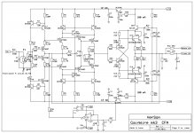
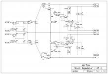
Here are the schematics (GainWire mk3 and Shunt Regulator +-15V) and the BOM.
When I receive the boards I prefer to assemble one bord and test it(it will take one week about) check for errors(I see some in silk screen now, but not functional) and then send to ones who ordered it, if you agree.
Damir
edit: be aware that the board contains two GainWire mk3 and two corresponding Shunt Regulators.
Attachments
Last edited:
Damir,why you are choosing this demon transistor that is out of production?
It is not easy to find replacement, and by the way LSK170 is in production but expensive. This jfet is very low noise but for this circuit it's no so important.
Maybe it could be used J112 or BF256B instead. For BF256 I can't find low voltage region Id Dds plot, and J112 looks quite OK.
Voltage drop on that CCS(J1 - 2SK170) is about 2.7 V and some jfet will not behaved as good CCS at so low voltage.
Diyaudio store offer the LSK170 A,B,C,D.
What is your recommendation?
B, correspond to Toshiba BL
I need one,one is your.
dadod------------2
platon.rado ----- 1
mlloyd1--------- 2
xrk971-----------1
reaper996--------1
Arthur-----------2
Tonza75-----------2
schillg11---------1
vac231-----------2
zrxshack----------1
dadod------------2
platon.rado ----- 1
mlloyd1--------- 2
xrk971-----------1
reaper996--------1
Arthur-----------2
Tonza75-----------2
schillg11---------1
vac231-----------2
zrxshack----------1
I remember one member (RCruz) suggested 2SK117GR as replacement for 2SK170 in GainWire mk2 power supply. Any feedback ?
I remember one member (RCruz) suggested 2SK117GR as replacement for 2SK170 in GainWire mk2 power supply. Any feedback ?
Yes, that one would be good too. Is this one in production?
Hi Damir,
Just noticed the thread - top class design, as usual.
Very clever bootstrapped output buffer.
"No distortion" line stage 😎
Cheers,
Valery
Just noticed the thread - top class design, as usual.
Very clever bootstrapped output buffer.
"No distortion" line stage 😎
Cheers,
Valery
Hi Damir,
Just noticed the thread - top class design, as usual.
Very clever bootstrapped output buffer.
"No distortion" line stage 😎
Cheers,
Valery
Hi Valery,
Thank you for your kind words, always a gentleman as usual.
BR Damir
Is there a way to use one stereo board with mods to be an unbalanced to balanced preamp?
There is always a way, but I don't see how to do that without increasing distortion to much or make it to complicate. I have to think more about it.
There is always a way, but I don't see how to do that without increasing distortion to much or make it to complicate. I have to think more about it.
OK, I did some simulation and my answer is no.
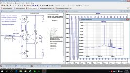
First what came to my mind is to use GainWire in inverting mode, I can connect two inputs +input and -input of two channels in parallel and the output will be balanced. To do that I need to use -input, but as this is CFA -input is low impedance so it needs some kind of buffer. That works but distortion increased 100 times(actually from 0.06 ppm to 5 ppm).
But there is another main reason why it would not work properly.
The gain in non inverting mode is calculated Rf/Rg +1 and in inverting mode Rg/Rf, that is inverting mode gain is non inverting gain-1. This is no problem for a power amp where a gain is set high in most cases around 28 times (it's important to know that balanced means balanced impedances and less symmetrical voltages) and difference is insignificant, but for preamplifiers a gain is low(in this case 3.6 times) and difference(non inverting - inverting gain) is not acceptable.
Adding external inverter buffer is other option but that is not GainWire any more.
Damir
It is not easy to find replacement, and by the way LSK170 is in production but expensive. This jfet is very low noise but for this circuit it's no so important.
Maybe it could be used J112 or BF256B instead. For BF256 I can't find low voltage region Id Dds plot, and J112 looks quite OK.
Voltage drop on that CCS(J1 - 2SK170) is about 2.7 V and some jfet will not behaved as good CCS at so low voltage.
Hi Damir,
regarding the substitution of the FETs i have following question.
is the J112 als sufficient to replace the 2N5486/85 or what else do you suggest? BF244 BF245 or J112. What are the key parameters for this FET?
Any proposal for the rectifier diodes, since you wrote in thee BOM only 1A
BR
Günni
Hi Gunni,
For those CCSs(J2 and J3) Idss should be around 10 to 15 mA and set to 8 - 10 mA. BF244B could be used, but no J112.
I left undefined the rectifier diodes, just 1 A. It could be used different types, normal, fast soft recovery, it is not critical. I use 1N4937.
BR Damir
- Home
- Amplifiers
- Solid State
- GainWire Mk3 CFA pre/phone amp with very low distortion