Power supply
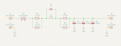
As I mentioned already, I want to use a very simple passive PSU for this amplifier - mainly to keep it simple and discrete, just like the rest of the project. Also, I don't want any power semiconductors in the PSU-section that would need cooling. For this reason, I want to go with a simple RLC-lowpass filter that smooths out any noise that may come from the external 24 V power-supply, and will provide each channel with its own filter to avoid crosstalk.
Schematic
Starting off, the core of the PSU is made up of two parallel resistors isolating the external power supply from the passive load of the RLC low-pass. While an inductive load should not be a big problem for the internal control-loops of most AC/DC converters, I don't want any risk for incompatibilities and oscillations. After that, the power inductor follows. This is a Murata 1400-series power inductor of 4.7 mH, capable of a DC of 600 mA. This should be just about perfect for this application without pushing the limits of the inductor too much. In parallel to the inductor, a flyback-diode is placed to avoid voltage spikes at switch-off. Another two parallel resistors follow between the inductor and the bulk capacitance, to avoid oscillations forming in this LC-network. The bulk capacitance is the last part of the circuit and provides a low-impedance voltage-source for the amplifier. To avoid large inrush-currents, a NTC is placed at the input of the filter network. The exact value of this has to be figured out, but this should be enough to avoid any damage to the amplifier or the AC/DC converter.
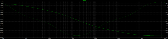
Simulation
The network should provide roughly 65 dB of attenuation at 1 kHz and over 100 dB at 10 kHz. With the high switching frequencies of well over 10 kHz of most power-supplies, as well as the PSRR of over 50 dB or so of the amplifier, this should avoid any audible coupling of PSU-noise onto the output of the amplifier.
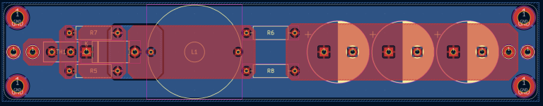
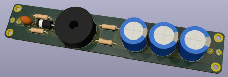
PCB
Just like the other PCB, this one has two layers with an (almost) solid ground plane on the bottom and large copper pours for the connections between the components. In the screenshot, the input is on the left. It directly connects to the NTC and then into the first bank of parallel power resistors. Each of these resistors can dissipate 2 W, so both of them result in a 2.35 Ohm resistor capable of 4 W dissipation. With a nominal dissipation of R*I^2 = around 0.59 W, this should be plenty of headroom to also cover current bursts due to inrush-current or fault conditions. At this point, the diode parallel to the inductor is also placed. The power-inductor follows, with its output feeding the second resistor bank. lastly, the bulk capacitance of 10 mF made up of three 3300 uF capacitors is connected.
The design of the PCB is again kept as symmetric as possible. To keep the amplifier reasonably thin, this PCB will lie on its side. Each channel will have its own PSU section, to avoid any crosstalk between the channels due to the passive PSU design. The symmetric PCB allows me to lie it on one side for the one channel and on the other side for the other channel, keeping the amp symmetric as a whole.
All in all, this is a really simple approach, but I think it will work well in this amp. I just want to see how simple an amp can really get while keeping good sonic performance, and am excited to see how all of this will work together.
As always, thank you for all the previous and future replies!
As I mentioned already, I want to use a very simple passive PSU for this amplifier - mainly to keep it simple and discrete, just like the rest of the project. Also, I don't want any power semiconductors in the PSU-section that would need cooling. For this reason, I want to go with a simple RLC-lowpass filter that smooths out any noise that may come from the external 24 V power-supply, and will provide each channel with its own filter to avoid crosstalk.
Schematic
Starting off, the core of the PSU is made up of two parallel resistors isolating the external power supply from the passive load of the RLC low-pass. While an inductive load should not be a big problem for the internal control-loops of most AC/DC converters, I don't want any risk for incompatibilities and oscillations. After that, the power inductor follows. This is a Murata 1400-series power inductor of 4.7 mH, capable of a DC of 600 mA. This should be just about perfect for this application without pushing the limits of the inductor too much. In parallel to the inductor, a flyback-diode is placed to avoid voltage spikes at switch-off. Another two parallel resistors follow between the inductor and the bulk capacitance, to avoid oscillations forming in this LC-network. The bulk capacitance is the last part of the circuit and provides a low-impedance voltage-source for the amplifier. To avoid large inrush-currents, a NTC is placed at the input of the filter network. The exact value of this has to be figured out, but this should be enough to avoid any damage to the amplifier or the AC/DC converter.
Simulation
The network should provide roughly 65 dB of attenuation at 1 kHz and over 100 dB at 10 kHz. With the high switching frequencies of well over 10 kHz of most power-supplies, as well as the PSRR of over 50 dB or so of the amplifier, this should avoid any audible coupling of PSU-noise onto the output of the amplifier.
PCB
Just like the other PCB, this one has two layers with an (almost) solid ground plane on the bottom and large copper pours for the connections between the components. In the screenshot, the input is on the left. It directly connects to the NTC and then into the first bank of parallel power resistors. Each of these resistors can dissipate 2 W, so both of them result in a 2.35 Ohm resistor capable of 4 W dissipation. With a nominal dissipation of R*I^2 = around 0.59 W, this should be plenty of headroom to also cover current bursts due to inrush-current or fault conditions. At this point, the diode parallel to the inductor is also placed. The power-inductor follows, with its output feeding the second resistor bank. lastly, the bulk capacitance of 10 mF made up of three 3300 uF capacitors is connected.
The design of the PCB is again kept as symmetric as possible. To keep the amplifier reasonably thin, this PCB will lie on its side. Each channel will have its own PSU section, to avoid any crosstalk between the channels due to the passive PSU design. The symmetric PCB allows me to lie it on one side for the one channel and on the other side for the other channel, keeping the amp symmetric as a whole.
All in all, this is a really simple approach, but I think it will work well in this amp. I just want to see how simple an amp can really get while keeping good sonic performance, and am excited to see how all of this will work together.
As always, thank you for all the previous and future replies!
Attachments

You might want to add a resistor in parallel with the inductor to prevent possible oscillation. 47ohms to 150ohms is what I typically use. Simulation will show best value for your LC resonance.
Hey everyone!
Sorry for the late update on the project. A few things delayed my progress, but I finally had some time to push the project forward again!
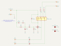
Turn-on delay board: schematic
With the amplifier being capacitively coupled, I knew I need some form of turn-on delay that only connects the outputs to the amplifier channels once the capacitors are charged to half the supply voltage, in order to avoid damaging ears or equipment with the loud turn-on "thump".
Keeping in line with the rest of the amplifier, I wanted to do this with a simple, safe and fully discrete circuit. I came up with the schematic attached below. A simple RC delay network (R3 and C1) is connected via a zener diode (D2) to the gate of a N-FET (Q1). Q1 is not conducting by default, meaning that as long as the threshold voltage of the zener diode is not reached and no voltage is applied to the gate, the relay (K1) is in its default state. In this state, the output capacitors (C2 and C6) are connected with small resistors (R1 and R2) to ground. This lets the capacitors charge quickly for as long as the RC-network is below the 15V or so that the zener diode needs to conduct. Once the threshold is reached (simulations show a delay of roughly 2-3 seconds, can be fine-tuned with R3) the relay switches and the amplifier outputs are connected to the headphone.
The input voltage to the board is assumed to be toggled between the 24V of the supply brick and ground. Therefore, once the amplifier is switched off, the diode parallel to the resistor responsible for the delay (diode D4) quickly discharges the delay capacitor C1 and switches the relay off within a few tenths of a second. This also means that if the switch is toggled between on-off-on quickly, the amplifier will still show the same turn-on delay.
All components are again standard through-hole components, hopefully making this board easy to build, repair and modify.
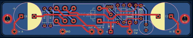
Turn-on delay board: PCB
The PCB of this board is meant to be laid on its side, as a lot of tall components (coupling capacitors, relay) would make the amp unneccesarily tall otherwise. For that reason, I tried to keep the board as narrow as possible and managed to get the width down to 20mm.
The board includes through-hole pads for the inputs, outputs, the switched voltage between 24V and ground and a dedicated ground pin. The bottom layer is mostly a solid ground plane with a few interruptions. I am not worried about those, as the board is fairly simple and the analog signals on there are large-signal and low frequency. I will keep it in mind for possible problems though.
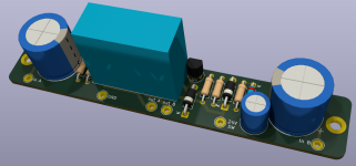
I finally ordered all the boards! The should arrive any day now. Once all the parts are here I will build up a first channel / PSU combination and see how it performs. Exciting stuff 🙂
As always I am looking forward to your comments!
Sorry for the late update on the project. A few things delayed my progress, but I finally had some time to push the project forward again!
Turn-on delay board: schematic
With the amplifier being capacitively coupled, I knew I need some form of turn-on delay that only connects the outputs to the amplifier channels once the capacitors are charged to half the supply voltage, in order to avoid damaging ears or equipment with the loud turn-on "thump".
Keeping in line with the rest of the amplifier, I wanted to do this with a simple, safe and fully discrete circuit. I came up with the schematic attached below. A simple RC delay network (R3 and C1) is connected via a zener diode (D2) to the gate of a N-FET (Q1). Q1 is not conducting by default, meaning that as long as the threshold voltage of the zener diode is not reached and no voltage is applied to the gate, the relay (K1) is in its default state. In this state, the output capacitors (C2 and C6) are connected with small resistors (R1 and R2) to ground. This lets the capacitors charge quickly for as long as the RC-network is below the 15V or so that the zener diode needs to conduct. Once the threshold is reached (simulations show a delay of roughly 2-3 seconds, can be fine-tuned with R3) the relay switches and the amplifier outputs are connected to the headphone.
The input voltage to the board is assumed to be toggled between the 24V of the supply brick and ground. Therefore, once the amplifier is switched off, the diode parallel to the resistor responsible for the delay (diode D4) quickly discharges the delay capacitor C1 and switches the relay off within a few tenths of a second. This also means that if the switch is toggled between on-off-on quickly, the amplifier will still show the same turn-on delay.
All components are again standard through-hole components, hopefully making this board easy to build, repair and modify.
Turn-on delay board: PCB
The PCB of this board is meant to be laid on its side, as a lot of tall components (coupling capacitors, relay) would make the amp unneccesarily tall otherwise. For that reason, I tried to keep the board as narrow as possible and managed to get the width down to 20mm.
The board includes through-hole pads for the inputs, outputs, the switched voltage between 24V and ground and a dedicated ground pin. The bottom layer is mostly a solid ground plane with a few interruptions. I am not worried about those, as the board is fairly simple and the analog signals on there are large-signal and low frequency. I will keep it in mind for possible problems though.
I finally ordered all the boards! The should arrive any day now. Once all the parts are here I will build up a first channel / PSU combination and see how it performs. Exciting stuff 🙂
As always I am looking forward to your comments!