Hi everyone!
This is my first post, so I hope everything abides by the rules and you get something out of it! This project was a long time coming for me and I would like to share it here.
I want to make a headphone amplifier, as I think it is a perfect "beginner project". Not too much power, not many unnecessary features, just a simple but performant amp. Going back to the basics if you will 😉
In this first post I will go over the background, some decisions I made for now and share the schematic I came up with.
Thank you all a lot in advance! I am really looking forward to your comments 🙂
Background and Goal
This amp is meant to deliver the best possible performance with the least amount of complexity and cost. Power efficiency is not a primary concern, as it is "just" a headphone amplifier, so naturally I chose a class A topology. The amplifier is meant to be built up entirely of through-hole components. While this makes it a lot nicer to build up for me as a hobbyist, it will also make the amp last a lot longer, as it will be easily repairable - especially as I am using only main-stream components (standard BJTs, standard values and packaging for resistors and capacitors). Furthermore, it is intended to feel premium and make a statement design-wise - audio gear has to look and feel premium as well imo. While the design is still a work in progress, I have some features in mind that I really want to implement. I want to show off certain parts of the electronics as a design-feature; more specifically, the power transistors in a TO-3 package. Therefore, the output-stage is designed in a way that there is only one high-power transistor - a MJ2955 BJT. That transistor was specifically chosen for its good availability and the TO-3 case available in a configuration with the collector connected to the case. The emitter-follower configuration of the output stage in combination with the grounded collector allows the case of the power-transistor to be grounded, which makes it possible to safely display it on the outside of the amp's case. I have always found old TO-3 packages to be really cool to look at and wanted a way to display them safely. I think this will be a really cool design-feature in the later amp!
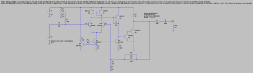
Schematic
Following the philosophy of simplicity and fully discrete design, the preamp-stage of the amplifier is kept relatively simple as well. The input stage consists of a long-tailed pair. The constant current source is set to a current of approx. 620 uA for a high input impedance (roughly 100 kOhm) of the two input transistors. This stage is followed by a common-emitter voltage amplification stage biased to roughly 2.6 mA. Finally, the power-stage is made up of a PNP-darlington pair in a common collector configuration. The amp is designed for a single voltage rail of roughly 20 V, so a bias-current of roughly 500 mA will flow through the output stage (with the DC-component of the output signal at half the supply voltage). The output is coupled with a large bipolar capacitor (how large exactly will be determined as well by some factors of the final design, but it will be somewhere between 3.3 and 10 mF; the simulations are done with the "best case" of 10 mF). This makes it possible to use a simple power-brick as a supply and therefore circumvent a lot of the headaches with regulation and safety when it comes to the higher grid-voltages. I plan on using a 24 V power-supply with a barrel connector (easy to get, cheap and safe) and filter the supply heavily to get a smooth 20V supply for the amplifier.
Projected Performance
The simulations done for now show a power output of >500 mW into 32 Ohms. The distortion is low (simulations show <0.0001% THD at 1 Vrms into 32 Ohms and <0.0005% THD at 0.5 W into 32 Ohms - both at 1 kHz). The simulated bode-plot shows plenty of phase margin and a flat gain curve (to within 1 dB) from 1.5 Hz to >200 kHz. The clipping behavior and power dissipation of the components seem decent. I am really happy with the schematic so far. To be clear: I know that simulations are just the first step and I fully expect the real-world performance to be worse, but the results encourage me to go further at least. I am curious to see what the real circuit can do!
Outlook
The next steps now are to build up a prototype and - if that works - design and order PCBs to populate. In parallel I am designing a suitable case. This will be a long project, so bear with me; I really want to push this amp to the best possible outcome. To this end, I would love feedback if you have some! I know some parts of this project may seem weird, but I really want to keep the single-PNP-output stage and just keep the whole thing simple and easy to build. I guess the spirit of this forum is to try new stuff after all 🙂
What do you guys think?
This is my first post, so I hope everything abides by the rules and you get something out of it! This project was a long time coming for me and I would like to share it here.
I want to make a headphone amplifier, as I think it is a perfect "beginner project". Not too much power, not many unnecessary features, just a simple but performant amp. Going back to the basics if you will 😉
In this first post I will go over the background, some decisions I made for now and share the schematic I came up with.
Thank you all a lot in advance! I am really looking forward to your comments 🙂
Background and Goal
This amp is meant to deliver the best possible performance with the least amount of complexity and cost. Power efficiency is not a primary concern, as it is "just" a headphone amplifier, so naturally I chose a class A topology. The amplifier is meant to be built up entirely of through-hole components. While this makes it a lot nicer to build up for me as a hobbyist, it will also make the amp last a lot longer, as it will be easily repairable - especially as I am using only main-stream components (standard BJTs, standard values and packaging for resistors and capacitors). Furthermore, it is intended to feel premium and make a statement design-wise - audio gear has to look and feel premium as well imo. While the design is still a work in progress, I have some features in mind that I really want to implement. I want to show off certain parts of the electronics as a design-feature; more specifically, the power transistors in a TO-3 package. Therefore, the output-stage is designed in a way that there is only one high-power transistor - a MJ2955 BJT. That transistor was specifically chosen for its good availability and the TO-3 case available in a configuration with the collector connected to the case. The emitter-follower configuration of the output stage in combination with the grounded collector allows the case of the power-transistor to be grounded, which makes it possible to safely display it on the outside of the amp's case. I have always found old TO-3 packages to be really cool to look at and wanted a way to display them safely. I think this will be a really cool design-feature in the later amp!
Schematic
Following the philosophy of simplicity and fully discrete design, the preamp-stage of the amplifier is kept relatively simple as well. The input stage consists of a long-tailed pair. The constant current source is set to a current of approx. 620 uA for a high input impedance (roughly 100 kOhm) of the two input transistors. This stage is followed by a common-emitter voltage amplification stage biased to roughly 2.6 mA. Finally, the power-stage is made up of a PNP-darlington pair in a common collector configuration. The amp is designed for a single voltage rail of roughly 20 V, so a bias-current of roughly 500 mA will flow through the output stage (with the DC-component of the output signal at half the supply voltage). The output is coupled with a large bipolar capacitor (how large exactly will be determined as well by some factors of the final design, but it will be somewhere between 3.3 and 10 mF; the simulations are done with the "best case" of 10 mF). This makes it possible to use a simple power-brick as a supply and therefore circumvent a lot of the headaches with regulation and safety when it comes to the higher grid-voltages. I plan on using a 24 V power-supply with a barrel connector (easy to get, cheap and safe) and filter the supply heavily to get a smooth 20V supply for the amplifier.
Projected Performance
The simulations done for now show a power output of >500 mW into 32 Ohms. The distortion is low (simulations show <0.0001% THD at 1 Vrms into 32 Ohms and <0.0005% THD at 0.5 W into 32 Ohms - both at 1 kHz). The simulated bode-plot shows plenty of phase margin and a flat gain curve (to within 1 dB) from 1.5 Hz to >200 kHz. The clipping behavior and power dissipation of the components seem decent. I am really happy with the schematic so far. To be clear: I know that simulations are just the first step and I fully expect the real-world performance to be worse, but the results encourage me to go further at least. I am curious to see what the real circuit can do!
Outlook
The next steps now are to build up a prototype and - if that works - design and order PCBs to populate. In parallel I am designing a suitable case. This will be a long project, so bear with me; I really want to push this amp to the best possible outcome. To this end, I would love feedback if you have some! I know some parts of this project may seem weird, but I really want to keep the single-PNP-output stage and just keep the whole thing simple and easy to build. I guess the spirit of this forum is to try new stuff after all 🙂
What do you guys think?
Attachments


Thank you for the response @lineup!
You're right, the resistor has to dissipate a lot of power. To make it capable of 500 mW into 32 Ohms, I will probably keep the 22 Ohms.
I plan to use a 10 W (should be a good choice with around 5W of nominal power) resistor that can be bolted to a heatsink, exactly as you mentioned!
You're right, the resistor has to dissipate a lot of power. To make it capable of 500 mW into 32 Ohms, I will probably keep the 22 Ohms.
I plan to use a 10 W (should be a good choice with around 5W of nominal power) resistor that can be bolted to a heatsink, exactly as you mentioned!
500mW is an awful lot.Thank you for the response @lineup!
You're right, the resistor has to dissipate a lot of power. To make it capable of 500 mW into 32 Ohms, I will probably keep the 22 Ohms.
I plan to use a 10 W (should be a good choice with around 5W of nominal power) resistor that can be bolted to a heatsink, exactly as you mentioned!
When I design headphone amps I test them at 3.162 mW and sometimes 10 mW.
I never go any further.
3.162mW is +10dB and 10mW is +20dB ... almost noone needs +20dB.
500 mW would make most headphone burn. And your ears would break.
You are right, the amplification factor is really quite high. I also agree that 500 mW is probably way too much for almost every application.
Both points in my view help the design be a bit more versatile though.
The amplification factor of roughly 5.7 (~15 dB) was chosen such that with an input of 1 Vrms (1.41 Vpeak) the output swing covers most of the supply voltage, 16 Vpp. I assume that 1.41 V is available from almost any source, and with this source the amp can be used "fully". This way, with volume controls, the amp will also be a very competent preamp and be suitable for high-impedance headphones (I only used 32 Ohms for the simulations, I want to use it with higher impedances as well).
The power of 500 mW will never be used, I guess I saw them mostly as "headroom". I also have to admit that I was "going with the flow" of the spec-sheet amplifiers that sometimes put out multiple watts 😉
I guess both the power and the voltage amplification is really only necessary for reeeeally specific applications.
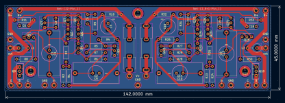
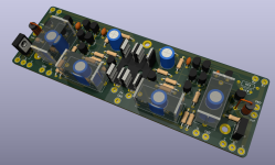
Designing the PCB
As I mentioned before, the next step is to test the circuit.
While this could be done with a breadboard-style test board, I decided to directly go to designing a PCB and have it manufactured professionally. I have had bad experiences with all the extra variables introduced by breadboard-style circuits and am reasonably confident that the circuit will (maybe with some persuasion and modification) work well.
Schematic
I used KiCAD, which I am very experienced with.
The circuit contains both channels. They are identical, and organized with the hierachical layout.
I added an optional RC filter which is intended to decouple the V+ supply of the signal-amplification stage from the output stage. This is done with R10 and C4. The values of them are more placeholders for now and can be bridged or placed depending on later measurements.
A snubber network and inductor at the output were included to avoid instabilities if the presented load on the amp is too capacitive. The value for the inductor seems to work well in the simulations but may need to be adjusted in the later amp. The snubber network did not seem necessary in the simulations, but may be placed if instabilities show up.
The footprints of the power components (power resistor and power BJT) are replaced with pads so that they can be placed directly onto the case, allowing adequate cooling.
Finally, I placed two capacitors in parallel for the input- and the grounding-capacitor in the feedback path. This way, builders of the amp can choose between an electrolytic capacitor (better low-end extension, lower cost) and a film capacitor (less low-end extension and more expensive, but possibly better audio quality). I know this is a polarizing topic, so I'd like to keep the choice to each person building the amp. 🙂
Layout
I aimed for a symmetric layout with the small signal components on the inner side of the PCB and the power components on the outer edges of the PCB. This should maximize the isolation between the two channels without making the board larger.
All signal and power traces were kept on the top layer of the PCB. This kept the bottom layer as an unobstructed ground pour for better shielding and solid return paths.
I am happy with how the PCBs turned out! I'll place an order soon and build up a first amp to test. I will keep you posted!
Attachments

It seems like I can't edit a post once it is fully up..
I found a small mistake and corrected the PCB, rendering and high level page of the schematic. They are attached here, sorry for the inconvenience 🙂
I found a small mistake and corrected the PCB, rendering and high level page of the schematic. They are attached here, sorry for the inconvenience 🙂
Attachments
I don’t think a TO-3 is needed given complexity of mounting and excessive size for a headphone amp.
Try something like a TTA004 from Toshiba. More than enough and easy to use and mount.
A critical aspect of SE class A headphone amps is how quiet the PSU is. Every bit of noise or hiss on that PSU will come through. Will need a regulated, filtered and probably a cap multiplier or low noise regulator to really clean it up to sub microvolt rms noise levels.
How you find the gain this schematic has? How to calculate it?It is true what @jxdking says. 32 Ohm headphones does not need any voltage gain.
You have x5.7 set by R8.
You could reduce R8 to 10k and so have only gain x2.
If you have other headphones like 300 or 600 Ohm, then you need some more gain.
The gain is
R9/R7+1
refering to schematic in post #9
R9/R7+1
refering to schematic in post #9
[...]
A critical aspect of SE class A headphone amps is how quiet the PSU is. Every bit of noise or hiss on that PSU will come through. Will need a regulated, filtered and probably a cap multiplier or low noise regulator to really clean it up to sub microvolt rms noise levels.
Perhaps a capacitor in parallel with R7 might reduce power supply coupling to the input. 22 uF would make a filter with a corner frequency of about 1.6 Hz, reducing 100 Hz ripple by 36 dB. Apart from that, PSRR is reduced in proportion to the amount of loop gain, which for this system would be non-trivial.
For power supplies feeding class-A amplifiers I've had good results with choke-input filters, which reduce noise easily as well as CRC filters, with the added advantage of having sinusoidal ripple current at a lower level through the first filter capacitors.
Thank you all for the interest!
As I mentioned in my first post, I also just love the TO-3 case visually. I connect it with vintage electronics and wanted to incorporate it into the case of the amplifier.
Regarding the power-supply, I want to keep it completely discrete and IC-free as well of course. As you mentioned @DSP_Geek I will try to power the amplifier with a combination of a LC-choke and RC filters with large bulk capacitors. My simulations show that this should give a really good performance with acceptable sag of the voltage rails.
True @xrk971, the TO-3 cased transistor is probably overkill. It will dissipate an average of roughly 5W, but I like the dissipation headroom and the good thermal connection of the TO-3 case. The TTA004 seems to be a really nice transistor though, I will keep it in mind for future projects. Thank you!I don’t think a TO-3 is needed given complexity of mounting and excessive size for a headphone amp.
Try something like a TTA004 from Toshiba. More than enough and easy to use and mount.
A critical aspect of SE class A headphone amps is how quiet the PSU is. Every bit of noise or hiss on that PSU will come through. Will need a regulated, filtered and probably a cap multiplier or low noise regulator to really clean it up to sub microvolt rms noise levels.
As I mentioned in my first post, I also just love the TO-3 case visually. I connect it with vintage electronics and wanted to incorporate it into the case of the amplifier.
This is also why I used a resistor instead of a PNP-transistor, @DSP_Geek. The PNP on the bottom end of the output stage can have a grounded case and can therefore be displayed on the outside of the amplifier safely. This would not be the case for a PNP on the upper side of the end-stage. It just felt wrong having one TO-3 power transistor on the outside while hiding the other one. Does that make sense? 🙂At not much more complexity a PNP current source could take the place of R22.
Regarding the power-supply, I want to keep it completely discrete and IC-free as well of course. As you mentioned @DSP_Geek I will try to power the amplifier with a combination of a LC-choke and RC filters with large bulk capacitors. My simulations show that this should give a really good performance with acceptable sag of the voltage rails.
- Home
- Amplifiers
- Solid State
- Fully discrete SE class A headphone amp