This is the original schematic (one channel):Conceptually yes, but as there is no schematic as far as I can see in that thread it's not really possible to tell if the implementation is the same?
Plus the cap multiplier:
And with all the other modules (PSU, attenuator):
As I wrote in the first post, I have already fixed the wrong connection in the cap multipier and as far as I checked mine they should provide the same operation (except the different OPAMP and the MOSFETs are from the original M3 design and not the lateral ones used by j4cbo).
Great advice, thank you! I'd like to eliminate the JFETs by any means.Side remark to the schematic in post 6, part "Op Amp Power" :
Q5.. and Q6.. are obviously intended as ripple filters, cap multipliers.
Now, the Fets wired as current sources try to push a fixed current
through bases of the bipolars - there is no other dc path. But the
base current is more or less fixed, consumption of the stage divided
by beta. This means the Fets can not work as intended, they will be
overdriven practically always. You will probably not notice this in
operation, because ripple suppression can still be "good enough".
This is a waste of fets. Better wire these as followers, establishing fet
darlingtons. Two or four additional resistors are required and can be
high-ohmic.
I am using the OPA1632 because it can take the +-10V supplied by my gamma3 DAC.there's probably a few issues, but let's back up a sec. for my dumb question.
first, what op amp are you actually using, the AD8139 or the OPA1632?
I'm asking because the AD8139 is a only a 12v part (as in +/-6V rails max)!
The drop is about 0.5V on each rail, so I get about +-9.5V on the OPAMPs. I could give you a more accurate number in the evening.Would be interesting to know the voltage drop in/out of this multiplier.
The precise number is not important; it would be good to see how
the device actually works, my guess is the fets are acting purely
resistive here. Please consider that 0.5V is the same or less than
the Vbe drop. You may want to check ripple suppression if possible.
However this is a side step only, no relation to your original problem.
the device actually works, my guess is the fets are acting purely
resistive here. Please consider that 0.5V is the same or less than
the Vbe drop. You may want to check ripple suppression if possible.
However this is a side step only, no relation to your original problem.
As far as I know the output voltage swing is going to be relatively low but tolerable. AMB told me it's going to be about 4Vp-p which should be fine with me. Since I didn't really get forward with my problem, I will try to run some SPICE simulations and see what it shows. Maybe it's easier than soldering for hours but if anyone has some ideas how to make the circuit working, don't hold it back 🙂
I think I found my nemesis and would need to do a proper job at the CCS circuits like matching the JFETs or getting different ones. This blog post was really informative: JFET cascode CCS comparisons
By using two questionable JFETs, MMBF5486, I might have messed up the whole purpose of the current sources. I will get back as soon as I get other ones and actually match them.
By using two questionable JFETs, MMBF5486, I might have messed up the whole purpose of the current sources. I will get back as soon as I get other ones and actually match them.
I have managed to build an LT-SPICE model of the amplifier. I can confirm that there was a huge amount of DC offset in the original design. However, when I changed the topology from sinking current into V- to sourcing current from V+ on the OUT+ side of the OPAMP (top branch of the circuit below), the output voltage offset got to zero. Here is the updated circuit in LT-SPICE:
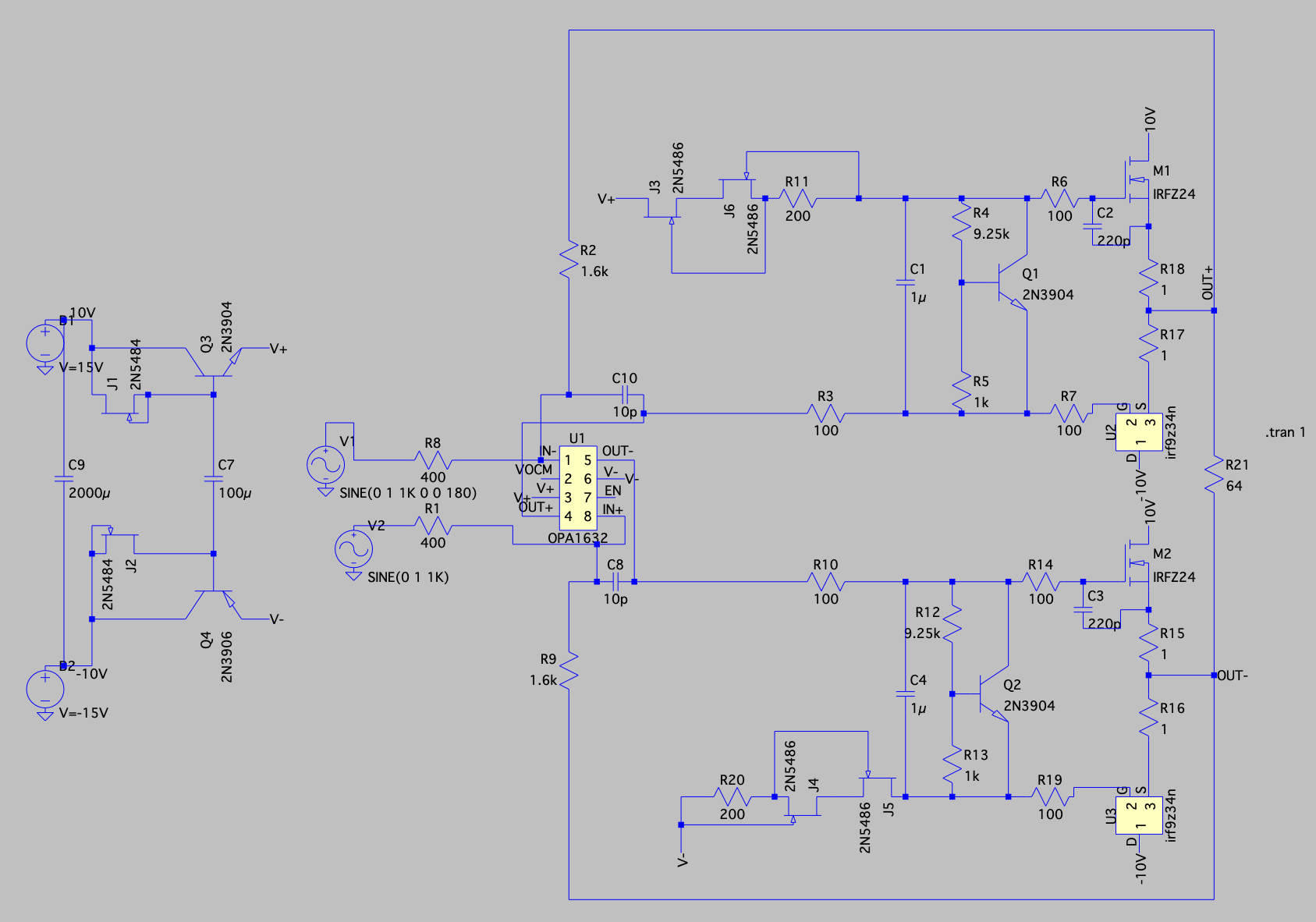
This is the first time I was running this software so forgive me please for the yellow OPAMP and MOSFET boxes. I adjusted the values of R11 and R20 so about 5mA current would flow into and out from the OPAMP. R4 and R12 were adjusted for 60mA quiescent current on the MOSFETs. The DC behavior of the circuit is just as I expected with zero hiccups. I don't think this is the case when I do the FFT analysis for the outputs if I set the input sine generators to 1V and 1kHz. Here is the spectrum for OUT+:
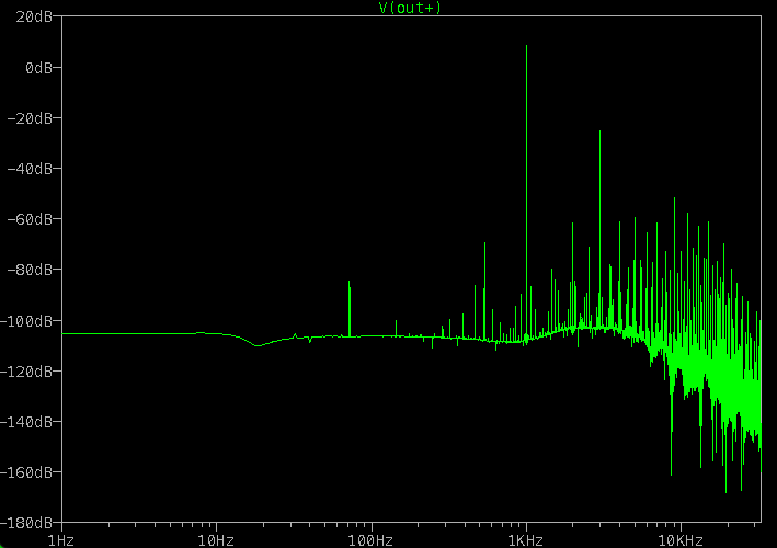
The 1st harmonic at 2kHz seems adequately suppressed with the 2nd hamonic at 3kHz only has a suppression of 35dB compared to the amplitude of 1kHz. I know that these models are not fully representing reality, but this seems a little too noisy for me. What do you guys think? Is this a spectrum expected in my circuit or is there something wrong with my simulation?
This is the first time I was running this software so forgive me please for the yellow OPAMP and MOSFET boxes. I adjusted the values of R11 and R20 so about 5mA current would flow into and out from the OPAMP. R4 and R12 were adjusted for 60mA quiescent current on the MOSFETs. The DC behavior of the circuit is just as I expected with zero hiccups. I don't think this is the case when I do the FFT analysis for the outputs if I set the input sine generators to 1V and 1kHz. Here is the spectrum for OUT+:
The 1st harmonic at 2kHz seems adequately suppressed with the 2nd hamonic at 3kHz only has a suppression of 35dB compared to the amplitude of 1kHz. I know that these models are not fully representing reality, but this seems a little too noisy for me. What do you guys think? Is this a spectrum expected in my circuit or is there something wrong with my simulation?
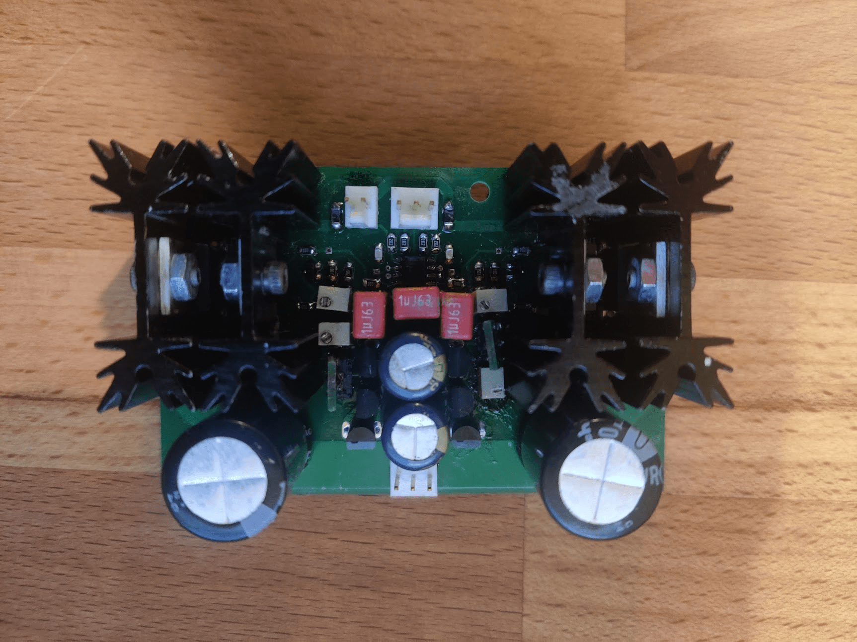
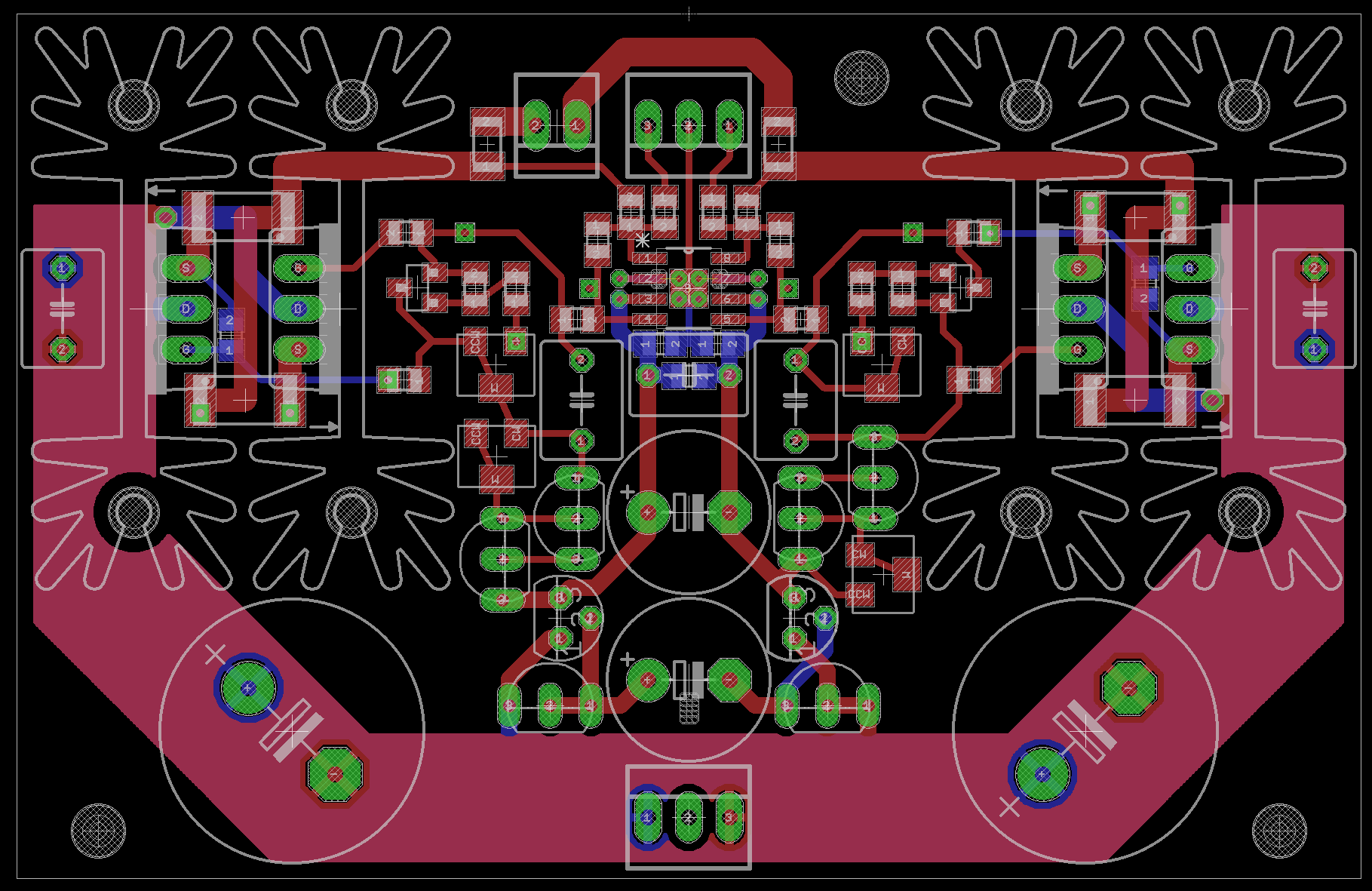
I am happy to announce that the circuit works and it produces music into my 64Ohm headphones 🙂 Now I need to build the second channel and then it's done. Here is a pic of the new module. I know It needs some cleanup and has way more through-hole transistors than I originally wanted. Unfortunately the JFETs were unavailable in SMD format at digikey (except the one for which I needed the adapter). For the JFET CCS setup, I followed this guide: https://www.preamp.org/static/cascoded-jfet-current-source/index.html
I ended up using J112 + 2SK209-BL for the CCSs. I set the OPAMP current to 4.5mA and the MOSFET quiescent current to 80mA. I hope it was worth the effort and this thing will perform better than the original AMB M3. I will post the results sometime next week.
If any of you need two PCBs to try this thing out, I am more than happy to send it to you. It costs about 100USD to build the two modules.
Looks good. Would love to hear what you think of the sound and how the finished board measures 🙂
I'd love to know how to measure the finished board 😀 Okay, to be fair, I'd love to have the equipment to measure it with. A laptop line-in probably doesn't suffice. Now that I think of it, I would need a differential line in.
Headphones !! I made an op amp car amp years ago using irfz40 and irf9z34. The amp easily pushed 40 w onto 4 ohms at 0.005 thd.
The principle is good but the power here is insane for headphones. Irf610 and 9610 are a much faster choice.
The principle is good but the power here is insane for headphones. Irf610 and 9610 are a much faster choice.
Yes, it's overkill if it's biased to like 1A quiescent current, but it's fine for 80mA. I followed amb.org's M3 design and didn't want to look into MOSFET options for now. I was looking at the lateral MOSFETs from Hitachi, but at 20USD a pair I passed. Many people consider the B22 amp from AMB the best of the best in DIY and that uses these irfz24 and irf9z34 MOSFETs, as well.
Well a full set of AP measurements would be nice, but that's actually not what I meant 😉 I was more thinking about measuring DC-offset (and if it is stable), measuring bias current (and if that is stable), checking for DC-spikes on turn-on/turn-off etc. - basically all stuff that you can do with a normal multimeter 🙂I'd love to know how to measure the finished board 😀 Okay, to be fair, I'd love to have the equipment to measure it with. A laptop line-in probably doesn't suffice. Now that I think of it, I would need a differential line in.
Oh, yeah, those I did measure. DC-offset is dead zero. Occasionally my multimeter shows 0.1mV. I set the bias current to 80mA and it was slowly decreasing as the amp was heating up. There was a slight audible spike when I switched the amp on, but barely noticeable. My M3 makes a much louder noise when switched on. It must be because of the higher gain. The M3 has a gain of 11 and this module has a gain of 2. I will post more results later this week when the parts arrive. Then finally my Gamma3 DAC + fully diff amp will be finished.
A line input will have two channels. Use one for each of the amp's outputs, and then diff them digitally after recording.I'd love to know how to measure the finished board 😀 Okay, to be fair, I'd love to have the equipment to measure it with. A laptop line-in probably doesn't suffice. Now that I think of it, I would need a differential line in.
And it's alive 🙂 and sounds amazing in my opinion. Thank you everyone for your input!
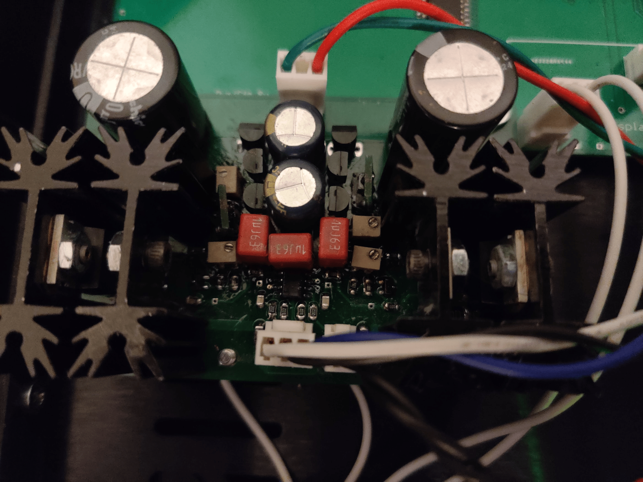
Here is one channel wired up:
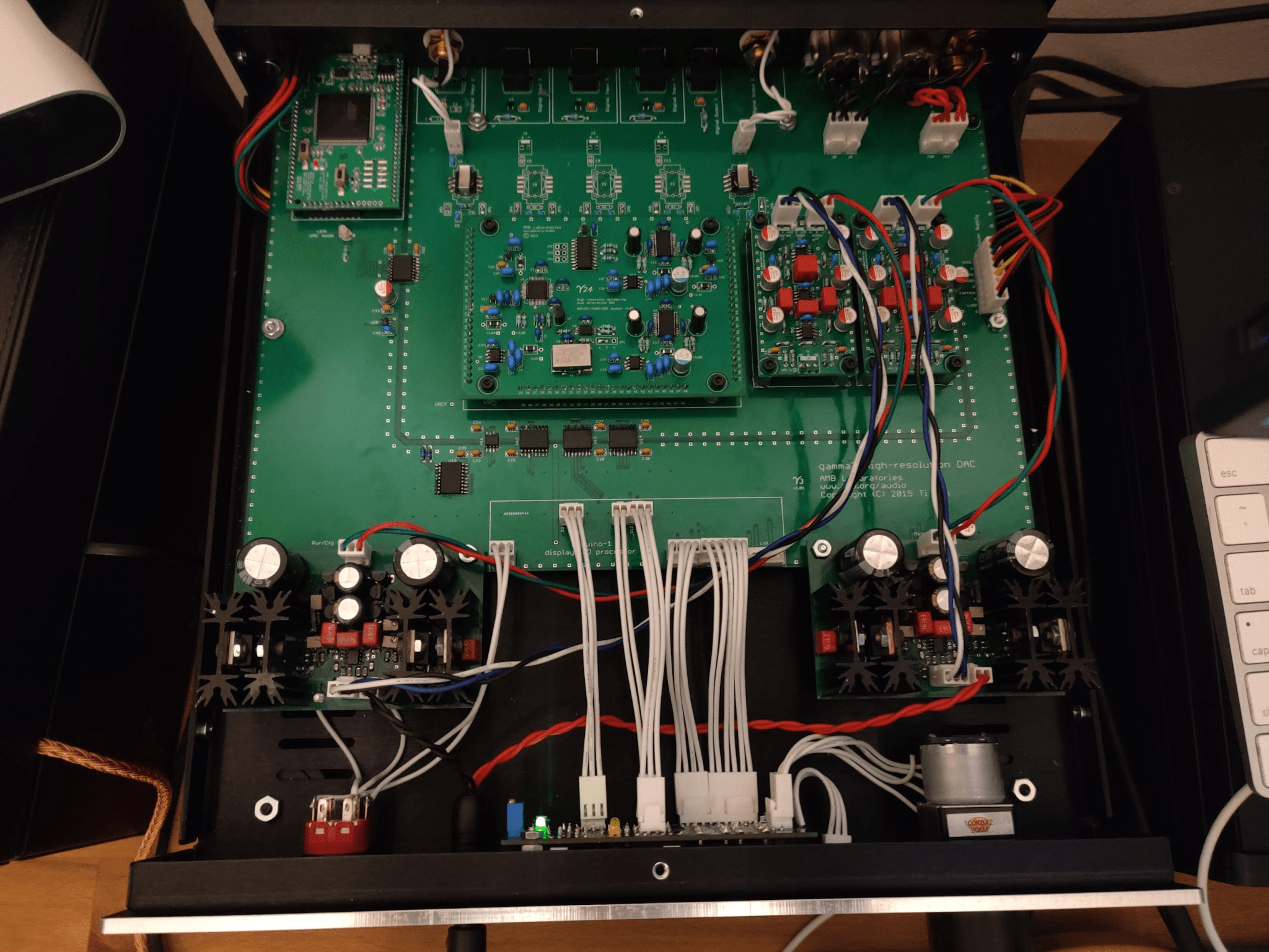
Here it is inside the AMB gamma3 DAC
Lastly, here it is from the front (sorry for the bad quality pic, the dark black and bright white are not the best to take a picture of):
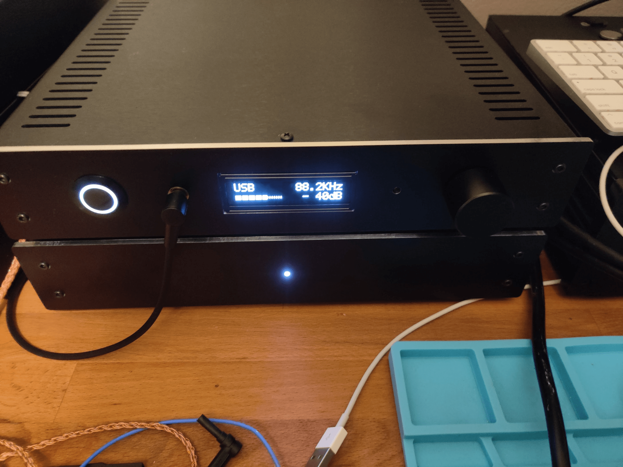
The amp is connected to a 4pin balanced 4.4mm pentaconn connector and finally to my Sony MDR-Z1R. The next step will be fixing the fluctuating noise on the LCDuino module which I cannot figure out where it's coming from. All the power rails seem to be noisy on the scope for some reason although I did the wiring correctly.
If anyone was interested, I could make a separate post about the finished setup.
Here is one channel wired up:
Here it is inside the AMB gamma3 DAC
Lastly, here it is from the front (sorry for the bad quality pic, the dark black and bright white are not the best to take a picture of):
The amp is connected to a 4pin balanced 4.4mm pentaconn connector and finally to my Sony MDR-Z1R. The next step will be fixing the fluctuating noise on the LCDuino module which I cannot figure out where it's coming from. All the power rails seem to be noisy on the scope for some reason although I did the wiring correctly.
If anyone was interested, I could make a separate post about the finished setup.
- Home
- Amplifiers
- Headphone Systems
- Fully differential hybrid OPAMP-MOSFET headphone amp