Dear Everyone,
Some of you are probably familiar with the works of AMB Labs. One of their project is called the M3 headphone amp which is a 3 channel hybrid opamp-MOSFET based headphone amp. It is a pretty decent amplifier which I have been using for 15years now. I decided to build a fully differential DAC which could directly drive a fully diff headphone amp (https://www.amb.org/forum/my-gamma3-build-with-a-built-in-fully-balanced-m3-amp-t4735.html) without issues with volume control and the low input impedance of the fully diff headphone amp. This is where my struggle began.
I found a design where a user on head-fi designed a fully diff amp based on the M3. He called it the M4: M4 head-fi link I decided that I wanted to put this into my Gamma 3 DAC until I get an AMB B22 or something similar done (there nothing similar I know, but I have something in mind).
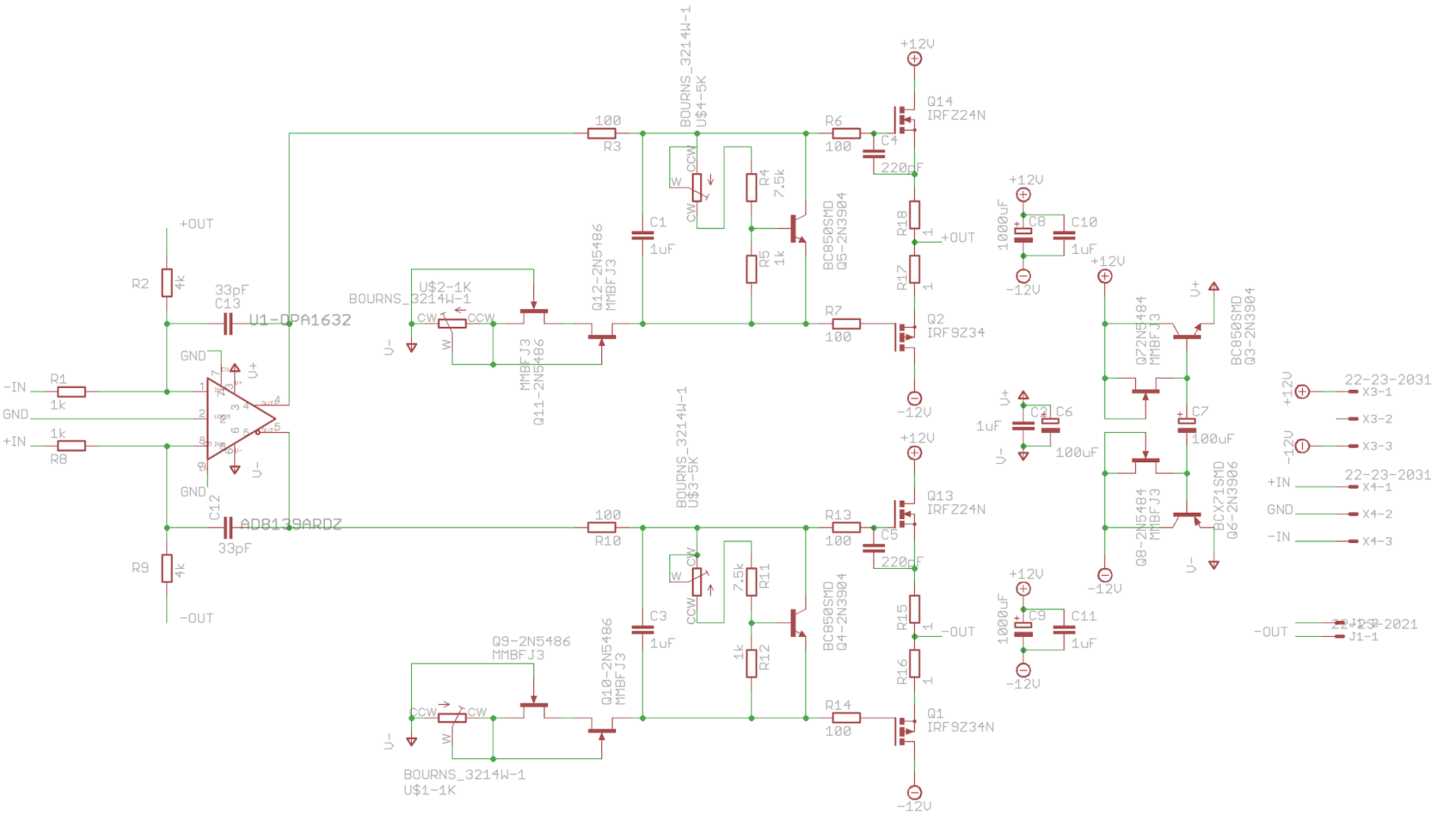
I designed and built the module but I cannot figure out what is wrong with it. I get stuck at the very first initial setup step where the opamp bias current needs to be adjusted. On one side of the differential amp, the one which has the positive input, everything seems fine. On the other side, the R5 resistor (R3 in my design) is stuck at 2.5V = 25mA no matter what I do. The trimpot U$2_1k has no effect on the voltage. If I remove the R3 resistor, the trimpot adjust the voltage on the JFET current source's leg (although it's not a current source at that time). When I removed the MOSFET stage from the amp, I got the same symptoms. I tried to bias the JFET current source (CW pin of U$2 trimpot) to the positive PSU_OPA (V+) instead of the negative, same result. When I removed the Q2 MOSFET bias transistor, the currents were the same and were correctly showing 0.5ish voltage on both R5 resistors (R3 and R10 in my design).
Could someone take a look at my circuit and the PCB design if some error is screaming at you instantly?
I already found the following issues, but resolving them didn't resolve the issue with the CSS or the fact that I couldn't force any current on the MOSFET:
One solution I was thinking about is to remove the two constant current sources because the JFETs have high tolerance with the Idss and probably ruins the symmetry but I don't know what would happen to the OPAMPs behavior if it was not biased to class A (AMB is saying that is the CSS for but I have never seen any other design having this feature).
Please don't bash on me for not knowing what I am doing. I already know that although I am trying to get up to speed with the fully diff opamp behavior and basic principles.
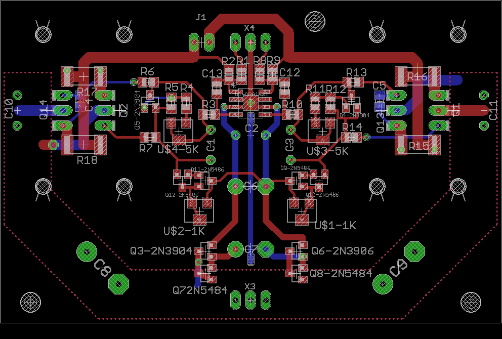
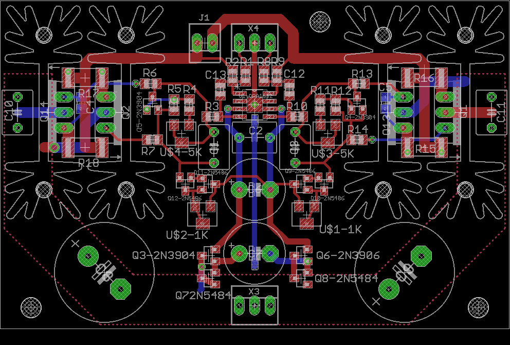
This is how the module looks like IRL (the PSU doesn't have a GND wire to avoid the ground loop, would come from the same GND as the balanced input):
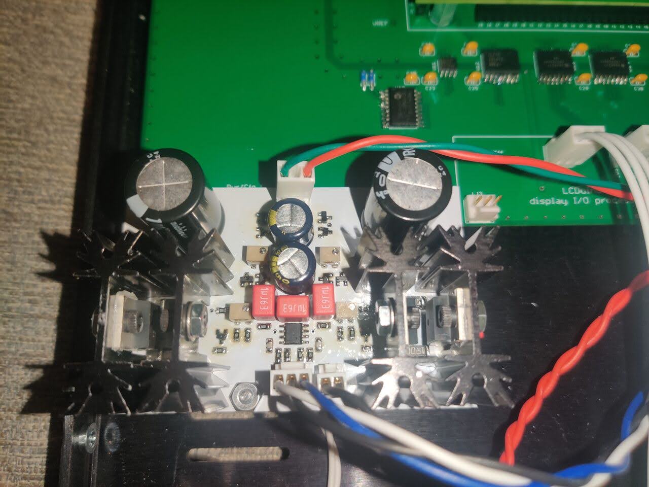
I would appreciate if someone could help me out. Also, after we find the error(s), if you are interested, I could send you a pair of PCBs for free so someone else could build this, as well.
Some of you are probably familiar with the works of AMB Labs. One of their project is called the M3 headphone amp which is a 3 channel hybrid opamp-MOSFET based headphone amp. It is a pretty decent amplifier which I have been using for 15years now. I decided to build a fully differential DAC which could directly drive a fully diff headphone amp (https://www.amb.org/forum/my-gamma3-build-with-a-built-in-fully-balanced-m3-amp-t4735.html) without issues with volume control and the low input impedance of the fully diff headphone amp. This is where my struggle began.
I found a design where a user on head-fi designed a fully diff amp based on the M3. He called it the M4: M4 head-fi link I decided that I wanted to put this into my Gamma 3 DAC until I get an AMB B22 or something similar done (there nothing similar I know, but I have something in mind).
I designed and built the module but I cannot figure out what is wrong with it. I get stuck at the very first initial setup step where the opamp bias current needs to be adjusted. On one side of the differential amp, the one which has the positive input, everything seems fine. On the other side, the R5 resistor (R3 in my design) is stuck at 2.5V = 25mA no matter what I do. The trimpot U$2_1k has no effect on the voltage. If I remove the R3 resistor, the trimpot adjust the voltage on the JFET current source's leg (although it's not a current source at that time). When I removed the MOSFET stage from the amp, I got the same symptoms. I tried to bias the JFET current source (CW pin of U$2 trimpot) to the positive PSU_OPA (V+) instead of the negative, same result. When I removed the Q2 MOSFET bias transistor, the currents were the same and were correctly showing 0.5ish voltage on both R5 resistors (R3 and R10 in my design).
Could someone take a look at my circuit and the PCB design if some error is screaming at you instantly?
I already found the following issues, but resolving them didn't resolve the issue with the CSS or the fact that I couldn't force any current on the MOSFET:
- MOSFETs are mirrored
- Capacitance multiplier is wired wront at the JFET
- VOCM on the OPAMP shouldn't be connected to GND
One solution I was thinking about is to remove the two constant current sources because the JFETs have high tolerance with the Idss and probably ruins the symmetry but I don't know what would happen to the OPAMPs behavior if it was not biased to class A (AMB is saying that is the CSS for but I have never seen any other design having this feature).
Please don't bash on me for not knowing what I am doing. I already know that
This is how the module looks like IRL (the PSU doesn't have a GND wire to avoid the ground loop, would come from the same GND as the balanced input):
I would appreciate if someone could help me out. Also, after we find the error(s), if you are interested, I could send you a pair of PCBs for free so someone else could build this, as well.
I do not completely understand the description of your problem. Is this a proven circuit ?
If it does not work then, the adjustment range may be too small due to parts tolerances.
Your description is not consistent, for example "Q2 MOSFET bias transistor" is an output
transistor. What does "MOSFETs are mirrored" and ".. multiplier is wired wront.." mean ?
Try to rewrite with parts numbers according to your schematic and add some dc voltages
in operation. Explain, what Q3, Q6, Q7 and Q8 are intended to do.
I did not look at the pcb layout. Of course, if it is wrong it can not work.
I think the idea is to merge the discrete buffer of the https://www.amb.org/audio/mmm/ (look under "schematic") with - more or less - the balanced input stage from the https://www.amb.org/audio/alpha24/ (look under "schematic"). It's a brilliant idea and I have been looking at something similar so kudos to @lampee for starting it - I will follow from the sideline for now 
I am sorry for the confusing response. Let me include the original schematic here:I do not completely understand the description of your problem. Is this a proven circuit ?
If it does not work then, the adjustment range may be too small due to parts tolerances.
Your description is not consistent, for example "Q2 MOSFET bias transistor" is an output
transistor. What does "MOSFETs are mirrored" and ".. multiplier is wired wront.." mean ?
Try to rewrite with parts numbers according to your schematic and add some dc voltages
in operation. Explain, what Q3, Q6, Q7 and Q8 are intended to do.
I did not look at the pcb layout. Of course, if it is wrong it can not work.
This is what I am trying to replicate with a fully differential OPAMP without the bass boost circuit (SbbL is short circuited). I will use the notation of this schematic in the followings.
- The OPAMP power circuit is a capacitance multiplier to separate the power of the opamp and the MOSFETs. In this circuit a virtual ground circuit (TLE2426) is used whereas I am using a symmetric power supply (AMB sigma 22 @ +-10V).
- The OPAMP circuit is a standard inverting circuit with global feedback having a gain of 11 here (5 in mine). There is a 33pF cap to set the bandwidth.
- The BIASOPL, Q3L, Q4L circuit is a.cascade JFET constant current source circuit (which I think is the issue)
- The Q2L circuit and the surrounding resistors is for setting the operating point of the MOSFETs.
First BIASOPL is set so the R5L resistor has 0.5V across it so 5mA current from the output of OPAMPL into Vop-. SInce the MOSFETs are basically open circuits at the gate the current will flow through R5L, R7L, BIASL, R6L, Q2L and the CSS circuit. Initially BIASL is set to its minimum (fully counter clockwise). In this case no current should flow through Q1L+ and Q1L-. Then BIASL is set while the voltage is checked across R9L- and the quiescent current of the MOSFETs is set to about 80mA, 80mV on R9L-.
The PCB design replicates the schematic for sure and shouldn't affect the DC behavior of the amp AFAIK.
As @Nisbeth was saying I am trying to merge the AMB lab's M^3 amps channels into one fully differential channel. This amp is originally 3 channels, two for L/R and one for ground which is a voltage follower circuit.
From what I understand about fully differential opamps, they really try to force the signal and its invert created from the input signal servoed around the mid voltage between the supply voltages or the VOCM if used. Since I am trying to draw positive current from both OUT+ and OUT- of the opamp, it might interfere with the OPAMPs behavior (handwaving argument, I know). I don't know if I should reverse the whole second stage in a way where the CSS circuit is connected to Vop+, has 2N5484 JFETs in it so current would flow into the OUT- of the OPAMP (still using the notation for the original amp here). I really don't know if this is a good idea or complete nonsense.
I actually had trouble sourcing the JFETs and it would be great if the CSS and the capacitance multiplier circuit could be changed to something which don't use MOSFETs. I bought them from an ebay vendor, but the cap multiplier circuit seems to be working fine. I have not measured the Idss of the JFETs nor do I know how that would influence the operation of the amplifier.
Why would you do that..? Or better... don't let that happen.
To answer your question (anyway)... you'd either open or close the Q2L fully - the same goes for the output MOSFET. Potentially, you'd be testing the current capabilities of your power supply (the output load would have its say here as well...). I suggest not doing that short
To answer your question (anyway)... you'd either open or close the Q2L fully - the same goes for the output MOSFET. Potentially, you'd be testing the current capabilities of your power supply (the output load would have its say here as well...). I suggest not doing that short
@Extreme_Boky Thanks, will not do that then  As I said I don't fully understand its purpose other than biasing the OPAMP to class-A. My goal is to check it somehow if the CCS circuit I have with the questionable JFETs is good or not. Measuring the Idss is not an option at the moment. SOT-23 seems a little too small to hook it up to a PSU which I don't have, although I could use the +-10V one. Hm..
I'm not sure this circuit will work as expected. One reason are quiescent voltages on the output.
An FDA will servo its output pins so that their CM voltage is at mid-supply or whatever voltage present on the Vocm pin. But the final output will have a lot of voltage offset. The feedback does not handle it, it will only care about the differential voltage. There will be a lot of DC voltage at each output, basically the Vgs of the main MOSFET.
This is fundamentally different from the regular opamp version where the feedback adjusts for the in-loop level shifting.
@lampee do you have the discrete buffer in the opamp feedback loop? Not sure if it causes any of the problems that you describe, but at least it is different from the original schematic. Also, I am not sure why you did not copy the complete A24 front end (= everything to the left of R14/R15 in the A24 schematic). Then you have a fully-working differential front-end and a fully-working discrete output stage to start from 
This circuit has worked for j4cbo here As long as there is no DC between OUT+ and OUT- (in my schematic), I'm good. There could be between them and GND but that is not connected to the headphones.I'm not sure this circuit will work as expected. One reason are quiescent voltages on the output.
An FDA will servo its output pins so that their CM voltage is at mid-supply or whatever voltage present on the Vocm pin. But the final output will have a lot of voltage offset. The feedback does not handle it, it will only care about the differential voltage. There will be a lot of DC voltage at each output, basically the Vgs of the main MOSFET.
This is fundamentally different from the regular opamp version where the feedback adjusts for the in-loop level shifting.
I didn't want to have global and local feedback loops at the same time. Also, I didn't want basically two alpha24s in my system. The A24 is in my gamma3 which will drive this headphone amp eventually. I don't think that the issue originates from the OPAMP stage.@lampee do you have the discrete buffer in the opamp feedback loop? Not sure if it causes any of the problems that you describe, but at least it is different from the original schematic. Also, I am not sure why you did not copy the complete A24 front end (= everything to the left of R14/R15 in the A24 schematic). Then you have a fully-working differential front-end and a fully-working discrete output stage to start from
I'm not sure what you mean by discreet buffer in the feedback loop. I don't have a local feedback for the opamp, just the global loop from the output back to R2 and R9.
I am not saying this circuit only worked only if there was no DC between OUT+ and OUT-. Also, when I measured the DC between OUT+ and OUT-, it was at 10mV as far as I remember. I can tolerate that and so could my headphones 
This circuitt worked as is (with a different OPAMP though). As far as I know the OPA1632 has an output buffer for each output. This is what its datasheet shows:
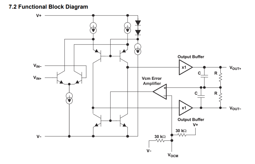
The OPAMP j4cbo used has the same functional block diagram.
This circuitt worked as is (with a different OPAMP though). As far as I know the OPA1632 has an output buffer for each output. This is what its datasheet shows:
The OPAMP j4cbo used has the same functional block diagram.
It is hard for me to understand you.This circuit has worked for j4cbo here As long as there is no DC between OUT+ and OUT- (in my schematic), I'm good.
I am not saying this circuit only worked only if there was no DC between OUT+ and OUT-. Also, when I measured the DC between OUT+ and
The OPAMP j4cbo used has the same functional block diagram.
@as_audio Sorry about that, I am trying. This circuit was originally designed by j4cbo (see the link). It worked for him, it doesn't work for me. I want it to work obviously and I don't understand why mine is not when the only difference is the OPAMP.
I think you were saying that there is going to be DC voltage on the outputs (OUT+ and OUT-) compared to GND (mid PSU rail), which I think it's fine until there is no DC between them.
I think you were saying that there is going to be DC voltage on the outputs (OUT+ and OUT-) compared to GND (mid PSU rail), which I think it's fine until there is no DC between them.
Conceptually yes, but as there is no schematic as far as I can see in that thread it's not really possible to tell if the implementation is the same?The OPAMP j4cbo used has the same functional block diagram.
Side remark to the schematic in post 6, part "Op Amp Power" :
Q5.. and Q6.. are obviously intended as ripple filters, cap multipliers.
Now, the Fets wired as current sources try to push a fixed current
through bases of the bipolars - there is no other dc path. But the
base current is more or less fixed, consumption of the stage divided
by beta. This means the Fets can not work as intended, they will be
overdriven practically always. You will probably not notice this in
operation, because ripple suppression can still be "good enough".
This is a waste of fets. Better wire these as followers, establishing fet
darlingtons. Two or four additional resistors are required and can be
high-ohmic.
- Home
- Amplifiers
- Headphone Systems
- Fully differential hybrid OPAMP-MOSFET headphone amp