I would still use a gate resistor on the lower mosfet.
Sorry about that , i've deleted it accidentally when updating the scheme. i have no intention of removing it. i have reattach the tested circuit. thanks again!
Attachments
What are your phase and gain margins?
Cheers,
Jeff.
I'm not sure how to find the phase margin...gain is 10X right?
thanks!
BTW, if you want to improve your CCS without stability issues, use a second MOSFET rather than an opamp:
I've also thought on this, but i'll need another matched transistor and another heat sink for it. so i've dumped the idea in favor of the op amp. The circuit simulates ok with the voltage reference , i'll give it a try and if i don't like what i'm hearing i'll try to improve it as suggested by you and other member.
thanks!
FYI, I had comparable issues during the design of my latest amp.
I remember, increasing VAS degeneration helped a lot in solving the stability issues.
I also did compare the 2sk216/2sj79 with the irf9610/710 combo. The irf sounded better, no matter what I changed regarding bias, degeneration...
Yesterday I had another audio lover visiting me, he really was impressed by the sound... Goosebumps
More info somewhere here:
https://www.diyaudio.com/forums/sol...low-nfb-fet-front-bjt-ops-13.html#post5916541
I've just started to read your thread. Thanks for the suggestions regarding alternative transistors and degeneration of VAS. i'll try them both!
I'm not sure how to find the phase margin...gain is 10X right?
thanks!
We're looking for the gain margin, rather than the gain. With a feedback loop the phase generally increases with frequency, and the gain generally decreases. If the phase ever gets to +180º when the gain is still above 0dB, you get oscillation.
However, because there are lots of other dynamics involved, you want to have some safety margins. A good rule of thumb is that you want to still have 45º of phase to go when you reach a gain of 0db (that's the phase margin), and be at least 6dB below 0dB when you reach 180º of phase (that's the gain margin).
You find these in SPICE by doing a small-signal AC simulation. I'm sure you simulator has something similar, but I'm not familiar with it.
I've also thought on this, but i'll need another matched transistor and another heat sink for it. so i've dumped the idea in favor of the op amp. The circuit simulates ok with the voltage reference , i'll give it a try and if i don't like what i'm hearing i'll try to improve it as suggested by you and other member.
thanks!
While I've never done a 2-MOSFET CCS, in a 2-BJT CCS the second transistor doesn't generally need heatsinking. And even if you don't match the MOSFETs for Vgs it will still be more stable than a voltage reference.
That being said, trying it with the simple voltage reference first is no bad thing.
Cheers,
Jeff.
Thank you JeffYoung for the "phase margin" explanation. So, I have to find the frequency at which the gain will became zero and also see the phase shift at that frequency. One problem is that i don't have a SPICE model for the IFN 146 and i used 2SK170 for simulations, but i'll try it anyway.
Indeed, now that you point it out, i figure that i can power the second CSS transistor from a 5 Voltage reference in which case it will dissipate very little power(10X less actually).
At this time my goal is to have a couple of these boards working ok as soon as possible(Christmas approaching fast!!!) and start doing listening tests.
after that, i'l start implementing the suggestions that you and others gave me and see what happens :
1. Differential vs single input
2. Increase the gate resistors
3. Adding a degeneration resistor to M11
4. Improving the CSS stability with another transistor
5. Changing the VAS transistors
6. Experimenting other values for the C7 capacitor
7. any other suggestions?
Indeed, now that you point it out, i figure that i can power the second CSS transistor from a 5 Voltage reference in which case it will dissipate very little power(10X less actually).
At this time my goal is to have a couple of these boards working ok as soon as possible(Christmas
approaching fast!!!) and start doing listening tests. after that, i'l start implementing the suggestions that you and others gave me and see what happens :
1. Differential vs single input
2. Increase the gate resistors
3. Adding a degeneration resistor to M11
4. Improving the CSS stability with another transistor
5. Changing the VAS transistors
6. Experimenting other values for the C7 capacitor
7. any other suggestions?
Found this on audioasylum. Haven't a clue how accurate it is.
On your list, (2) is mostly for added stability. See how it affects your phase and gain margins.
For (7), try cascoding your VAS. It will hugely decrease the Early effect distortion (by making the voltage drop across the VAS gain device much smaller).
.model 2sk146 NJF(Beta=75.04m Rs=1.116 Rd=1.116 Betatce=-.5 Lambda=689.7u
+ Vto=-.5038 Vtotc=-2.5m Cgd=46.53p M=.3541 Pb=.3905 Fc=.5
+ Cgs=69.32p Isr=104.7p Nr=2 Is=10.47p N=1 Xti=3 Alpha=10u Vk=100
+ Kf=21.36E-18 Af=1)
*$
On your list, (2) is mostly for added stability. See how it affects your phase and gain margins.
For (7), try cascoding your VAS. It will hugely decrease the Early effect distortion (by making the voltage drop across the VAS gain device much smaller).
actually the 2SK216 is becoming linear (with 25mA load) only after 20V Drain Source voltage. so i can reduce the dissipated heat only by a factor of 2.5 XIndeed, now that you point it out, i figure that i can power the second CSS transistor from a 5 Voltage reference in which case it will dissipate very little power(10X less actually).
actually the 2SK216 is becoming linear (with 25mA load) only after 20V Drain Source voltage. so i can reduce the dissipated heat only by a factor of 2.5 X
We're reaching the edge of my knowledge here, but I don't think you care about that. The local feedback between the two is what's going to linearise the current source.
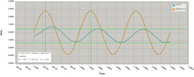
i've done the phase shift simulation,
at 1MHz, the output is approaching to a 45º phase shift, and the gain has decrease from 10X to 4.6X. have no idea how to interpret this 🙂
at 1MHz, the output is approaching to a 45º phase shift, and the gain has decrease from 10X to 4.6X. have no idea how to interpret this 🙂
Attachments
Last edited:
Something's not quite right; that's showing Vout smaller than Vreference. (I assume Vreference is the input?)
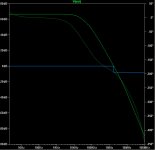
Also, if that's the best the CircuitLab can do, then it's time to download LTSpice (it's free). This is the output of the small-signal AC analysis in LTSpice. The solid green line is the gain; the dotted green line is the accumulated phase angle. You can see that over the audio range the gain is about 65dB.

I drew the blue lines. The top one shows where the gain line crosses 0dB (at about 1MHz). If we then draw a vertical line to the phase line and then over to the phase axis (lower blue line), we get about 190º. That's over 180º, so this circuit is unstable and will oscillate.
To have a 45º phase margin, the accumulated phase angle would need to be 135º.
To find the gain margin, you go backwards. Draw a horizontal line where the accumulated phase crosses 180º, draw a vertical line to the gain line and then over to the gain axis. You want this to be -6dB or lower.
In the above chart it's going to be about +5dB, again indicating that this circuit is unstable.
(Note that you don't actually have to draw the blue lines. If you control-click the trace label LTSpice will add a cursor and a window which reads out all the pertinent values.)
Cheers,
Jeff.
Also, if that's the best the CircuitLab can do, then it's time to download LTSpice (it's free). This is the output of the small-signal AC analysis in LTSpice. The solid green line is the gain; the dotted green line is the accumulated phase angle. You can see that over the audio range the gain is about 65dB.
I drew the blue lines. The top one shows where the gain line crosses 0dB (at about 1MHz). If we then draw a vertical line to the phase line and then over to the phase axis (lower blue line), we get about 190º. That's over 180º, so this circuit is unstable and will oscillate.
To have a 45º phase margin, the accumulated phase angle would need to be 135º.
To find the gain margin, you go backwards. Draw a horizontal line where the accumulated phase crosses 180º, draw a vertical line to the gain line and then over to the gain axis. You want this to be -6dB or lower.
In the above chart it's going to be about +5dB, again indicating that this circuit is unstable.
(Note that you don't actually have to draw the blue lines. If you control-click the trace label LTSpice will add a cursor and a window which reads out all the pertinent values.)
Cheers,
Jeff.
Attachments
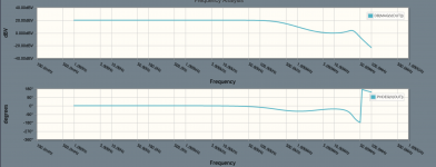
It was my fault, the software has the frequency analyzer tool, it was me who did not know how to use it. Thanks for the explanations Jeff Young. I've attach to screen shots of the simulation. It seems that the phase will approach 180 at 50MHZ and -6.8db.
Please note that the simulation was done with 2Sk170 and not IFN146.
Please note that the simulation was done with 2Sk170 and not IFN146.
Attachments
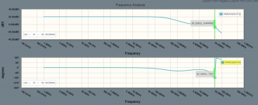
Yep, so your gain margin is about 7dB (that's sufficient).
Your gain crosses the 0 line at about 10MHz; the lowest the accumulated phase goes before that looks to be about 70º, so your phase margin is about 110º (that's gobs).
Your gain crosses the 0 line at about 10MHz; the lowest the accumulated phase goes before that looks to be about 70º, so your phase margin is about 110º (that's gobs).
Yep, so your gain margin is about 7dB (that's sufficient).
Your gain crosses the 0 line at about 10MHz; the lowest the accumulated phase goes before that looks to be about 70º, so your phase margin is about 110º (that's gobs).
Thanks for the detailed explanation JeffYoung! i finally understand the use of this .
It's the first stage(out of two in my case: Front Stage & Output Stage) of a class A power amplifier.What is the purpose of this circuit?
something like this.
It's the first stage(out of two in my case: Front Stage & Output Stage) of a class A power amplifier.
something like this.
I looked at last pdf file you posted. There is no gate stopper resistor in series with the gate of M10 despite prompts to include such by commentators.
You need to do this if there is any length of wire connecting to the gate of the MOSFET. Without them you are inviting oscillation.
Also you have a relatively low impedance path through R53 to the common connection the BC550 transistors so if oscillation occurs this will feed back through the positive supply rail.
The level of current passing through R53 will also be excessive with regard to the level of base current required by such high gain transistors. You should look into increasing the values of R53 and R54 to put them into a better scale.
Furthermore the Vceo breakdown rating of BC550 is 45 volts max whereas your rail voltage is 56 volts. BC546 would be a better choice.
With regard to stability the point where the angle of slope reaches - 45 degrees lies where the gain has reduce from what level it was at 1Hz to .707 equalling - 3dB.
You need to reckon what the matching frequency is at that point.
Changes happen at a faster rate relative to the decline in gain and start a decade in frequency lower than the - 3dB frequency point.
Since simulations represent ideal rather than real world situations you should aim a bit lower than what a decade of frequency difference could be in your compensation.
I looked at last pdf file you posted. There is no gate stopper resistor in series with the gate of M10 despite prompts to include such by commentators.
It was a type on the schematics, I never removed it from the actual board. I have reattached the schematic.
Also, you have a relatively low impedance path through R53 to the common connection the BC550 transistors so if oscillation occurs this will feed back through the positive supply rail.
The level of current passing through R53 will also be excessive about the level of base current required by such high gain transistors. You should look into increasing the values of R53 and R54 to put them into a better scale.
Good spotting!! Fortunately, a keen sense of smell can sometimes compensate lack of experience. I've smelt it immediately after powering the amplifier. I changed the values for those two resistors to 10K each.
Furthermore, the CEO breakdown rating of BC550 is 45 volts max whereas your rail voltage is 56 volts. BC546 would be a better choice.
I used it because I had no cheap transistor with Vceo or Vds greater than 65V and I have around 20 pieces of it. I also know that moving the most of the 56V drop to the cascading transistor would improve the performance of the IFN transistor. Since both IFN 146 and BC550 allow for a maximum 40V drop I decided to play safe and split the 56V between the two, and so I used same value for the two resistors discussed above R53 & R54.
With regard to stability the point where the angle of slope reaches - 45 degrees lies where the gain has reduced from what level it was at 1Hz to .707 equaling - 3dB.
You need to reckon what the matching frequency is at that point.
Changes happen at a faster rate relative to the decline in gain and start a decade in frequency lower than the - 3dB frequency point.
I got rid of the HF oscillations as soon as I ‘ve removed the OpAmp. At this point I only have some small bias stability issues and external oscillations. Left speaker has a little buzz all the time and stops the moment I touch the speaker cable connector and the right speaker is the exact opposite: it’s quiet and start buzzing only if I touch the speaker cable connector. Also changing the position of my 3.5m speaker cable around the house changes the way it buzzes. Buzzing frequency varies between 20Hz to 400HZ, with a predilection for 50HZ. It may be because on the left board I have a capacitor around the R54 resistor. I’ll switch the speaker cables and I’ll find out.
Loud noise if the speaker’s cable is connected and remove or attach the RCA cables.
Nevertheless, at this stage the amplifier is quite ok for listening test and I notice that the more I use it the better it is. The bias is wondering far less< 20mV and the buzz is nearly audible whereas in the first day it was quite loud. I did nothing during this time just powered it.
I have a list of suggestions to try out, it’s just at the moment the sound is changing from one day to another and will make any test irrelevant. I’ll just powered it for 100+ hours and only then I’ll start trying new things.
Attachments

Last edited:
- Home
- Amplifiers
- Solid State
- Front Stage oscillating problem