Well, the transistors weren't too bad in the end, though I'm still not convinced about some of the ground plane solder joints which are an absolute pain on these boards. Anyway, I've used the meter and it tells me I have continuity and no unexpected resistances so I've started to install the boards with a view to powering them up.
Ray
Ray
Good luck.
Keep us posted.
Strange that Siliconray does not even reply to our concerns...
BR
Eric
Keep us posted.
Strange that Siliconray does not even reply to our concerns...
BR
Eric
Well, both boards installed and powered up. As they're both behaving the same I'm assuming my fears about potential dry joints were a little pessimistic (but the boards are still dogs to solder!).
Anyway, I've set bias for 200mA on both and its rock steady.
The problem I have is the DC offset. Both boards are showing very similar values around 0.45V. It was reducing nicely but I ran out of travel on the presets. I used 200 ohm presets as per the schematic but I guess I'm going to have to swap them out for 500 ohm presets (not looking forward to modifying these boards).
On re-reading the thread I noticed SiliconRay mentioned 500ohm presets in post #55; these sort of inconsistencies are unhelpful so I think, when I finish, I'll post a reference parts list (BOM) from my build.
Yep, that did it, just replaced R13 with 200R; 0.02V DC offset now and holding steady. One board done, another to go then, maybe, some music.
Ray
Ray
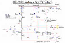
Revised schem based on comments in thread
Hi Ray,
I went through the whole thread and modified the schematic based on issues people had found building this headphone amp, the most common issue seems to be some oscillation and this appear to have been resolved by the addition of a 15pF across B-C of Q3. I do not own the headphone amp. I just hope if can help future builder.
BR,
Eric
Attachments
Last edited:
Thanks Eric. As I don't want to be forever putting the boards in and out your schematic prompted me to try the first channel that I changed the resistor in before proceeding to the second.
So, I connected the R output directly to the DAC buffer and the L output through the JLH board, accepting that there would be a big imbalance in levels between L & R.
The result (L output); it plays music cleanly and actually sounds quite nice. Bias was rock steady and DC offset was down around 0.01V with only tiny variations so things are looking good. That is without the 15pF cap across Q3 so, arguably, it worked first time.
There's always a but though isn't there. I have a low level hum via the JLH board. The level of the hum doesn't change with volume setting and I'm sure it's grounding related so work to do in that respect (I'm now having niggling thoughts about those ground pads that were such a pain to solder on the PCB). I have no hum on the R output so it's definitely JLH board related.
Next step is to change R13 on the second board and test and commission it so I can compare the two channels and see what the overall troubleshooting picture looks like.
Ray
I was about to work on changing R13 on the second board when I noticed I hadn't secured a ground connection. Now, with it screwed down properly almost all of the hum has gone, just a tiny residual level left for another day!
Onwards.
Ray
Onwards.
Ray
Nice work.
In order to avoid having to build a power supply with mains (100-240Vac) inside the enclosure, I have found this nice +/- 12Vdc, 1A dual supply that works with a single DC input. Power input could be a from a laptop supply, ex 19V, 4A.
See here : Dual 12V Power Supply Mini Board
At $15 USD including shipping it's a safe bet. I just wonder if the LM2575T regulator is noisy ?
BR,
Eric
Success!
Swapped R13 on the second board and reinstalled, set offset and bias and both boards behaving similarly and no significant drift encountered so plugged in the laptop source and a pair of headphones and had a listen.
The verdict? What a super little amp! great sound, even with no real burn-in, lots of subtle details coming through, nice and smooth but with weight and attack when required.
Oh, and I've sorted the grounding and the amp is nice and quiet now too.
I didn't use onboard heatsinks for the output transistors, instead bolting them to the bottom of the chassis, which is a substantial piece of aluminium, 3mm thick - it barely gets warm. I'm running 12V supplies and 200mA bias.
For completeness, I'm driving the amps from a Curryman DAC (Sabre ES9023) and DIYINHK USB board combination, via a TKD volume pot. All power supplies are based on the recent Curryman DAC/PSU group buy. The power supplies for the amp boards get a little warm. I've linked to a couple of pictures of the project below.
SiliconRay, many thanks for the free PCBs. The amplifier worked first time but I think you could improve the boards to make it an easier project to work on by making some of the pads larger and slightly further spaced apart as hand soldering it is a bit of a challenge! It would also help if there was a definitive schematic and parts list (that agree with each other).
Ray
An externally hosted image should be here but it was not working when we last tested it.
An externally hosted image should be here but it was not working when we last tested it.
R11?
I got my cards and have started to solder the components. For R11 I got a 0 ohm resistor instead of the 10k, I wrote a question to siliconray about it, he claims it is supposed to be that way but I am not convinced. What do you say guys, is R11=0 OK.
I don't understand the theory aboat the current source.
/S
I believe R11 can't be zero ohm.
This current source will varie from about 0.65V/522 to 0.65V/22 so 1mA-30mA
Both variable resistors should be 500ohm according to SiliconRay.
I'm also thinking about building one but I don't have a decent pairs of cans so it would be more for fun...LOL
BR,
Eric
This current source will varie from about 0.65V/522 to 0.65V/22 so 1mA-30mA
Both variable resistors should be 500ohm according to SiliconRay.
I'm also thinking about building one but I don't have a decent pairs of cans so it would be more for fun...LOL
BR,
Eric
Last edited:
I got my cards and have started to solder the components. For R11 I got a 0 ohm resistor instead of the 10k, I wrote a question to siliconray about it, he claims it is supposed to be that way but I am not convinced. What do you say guys, is R11=0 OK.
I don't understand the theory aboat the current source.
/S
Here's the parts list I used for my build, which works well (see a few posts back).
Ray
R2 47K 0.25W
R3, R5, R12 4.7K 0.25W
R6 220R 0.25W
R8 2.7K 0.25W
R9 200R 0.25W
R10 0R51 1W
R11 10K 0.25W
R13, 14 22R 0.25W
R15 10R 0.5W
VR1, VR2 200R
C1 1uF
C2 330pF
C6, C7 4700uF
C6a, C7a 100nF
Q1, Q2 BD937
Q3 BC550
Q4, Q5, Q6, Q7, Q8 BC560
Last edited:
Thank you guys, I think it would be overload on Q5/Q6 with R11=0 OhmW where did you get hand of the BD937's? I can't find them at Farnell, Mouser etc.
Thank you guys, I think it would be overload on Q5/Q6 with R11=0 OhmW where did you get hand of the BD937's? I can't find them at Farnell, Mouser etc.
I got my BD937 devices here;
LittleDiode - Electronic Components Supplier
Good luck with your build.
Ray
I have build the schematic that was pointed @ 86th post.
Works, everything is stock except outputs --> TIP41 is used.
Oscillates without 15pF capacitor. Soldered 20pf there.
Bias is rock solid 200mA, but DC drifts some times... the problem could be my layout, all transistors are almost tied together 😀
Using ATH-A900 metal blue closed cans, 40ohm imped. per driver.
This schematic drivers them very well, "slam, attack, notes, everything is there"
Could it be possible to lower the gain just by reducing feedback resistor to a lower one ?
DC drift was caused by dirty contacts on solder joints where probes were connected.
Changed the feedback resistor "output to Q1 emitter" from 2.7k to 1k.
Changed Q1 emitter to ground resistor from 220R to 470R
This gain now is perfect for 40R ATH-A900 closed alu. cans. Input around ~0.9V and with the volume max i get no noticeable distortion(clipping or some sort of unpleasant sound).
I all ready enjoy the sound though there is only one channel playing. Best listening is at low volumes 😀
Transistors are all stocks = BC560B x5 and BC550B x1
Outputs 2xTIP41C HFE 47 matched.
Iq is set to 160mA, DC offset sits @ 000.0mV for TEN minutes straight.
Power is coming from laboratory PSU, so there is room to make a small improvement on the sound.
Hi,
How is the slam, attack with the new feedback resistors ?
Just wondering because before the Gain was 2700/220 so 12.3 and with your value of 1000/470 only 2.1 so the overall global feedback is greatly reduced therefore increase distorsion and lower damping factor.
Now sure if headphone's speakers are affected by lower damping factor, your feedback would be appreciated.
Why did you lower your bias from 200mA to 160mA, did your TIP41C overheated ?
I'm glad my updated schematic was helpfel to someone 😉
Thank you,
Eric
Last edited:
No, alu. radiator i use is decent and has very good passive cooling capability.Why did you lower your bias from 200mA to 160mA, did your TIP41C overheated ?
Its from "high end computer PSU block" 😀
BOTH TIP41C-s are on the same heat sink also.
I lowered it because i don´t see the point having so much current. With ATH-AD900 cans, 160mA Iq and 2.1 gain, i couldn´t see outputs leaving A-class. Voltage from Creative SB570 card was about 0.9V.
I measured currents on both side with multimeter´s, steady with or without load/max volume.
Is there a risk by lowering the gain the distortion will be increased, what might the percentage be ?
How is the slam, attack with the new feedback resistors ?
One channel only and i all ready feel it has the potential(12.3 gain)
With (2.1) at first listening i could´t make a difference -> ONE CHANNEL ONLY.
I will comment on this when i get two boards ready and steady!
I remember very good, when i had Sound Blaster X-Fi HD - Sound Blaster - Creative Labs (United States)
There was a lack of ASIO2.0 codecs, sold it.
The sound from the headphone jack with ATH-A900... gorgeous.. i never forget what i heard/experienced with that type of USB DAC/headphone amplifier.
I will make pictures tomorrow and hopefully get the 2nd channel done by that time. Actually i need to solder together 2 more channel, make them compact as possible.
I will be driving JHL with Texas active volume control... all these components i must somehow fit into standard case of satellite television tuner 😀.
Renu
- Status
- Not open for further replies.
- Home
- More Vendors...
- Siliconray Online Electronics Store
- ★★Free JLH Hifi Headphone Amp PCB, 0.008% THD★★