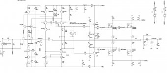
Put ~1meg here.
Don't keep that node unloaded!
This will eliminate real construction difference from model in terms of open-loop gain difference due to PCB leaks difference and the need of deep ultrasonic clearing!
And 10+10pf really are very much and will impact on slew rate and widebandness. Keep in mind, your IPS current is the only one to recharge this capacitance.
Last edited:
Thank you BesPav
What about ips jfet source resistors.... should I reduce those or even eliminate it's resistance ?
What about ips jfet source resistors.... should I reduce those or even eliminate it's resistance ?
What about ips jfet source resistors.... should I reduce those or even eliminate it's resistance ?
Shunt them with something shielded (or place 2 inductances in zigzag line on pcb) and set that LR freq slightly upper audioband.

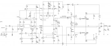
Trying to increase OLG by increasing IPS gain so having better THD I doubled the input jfets.
To avoid jfet interactions without using large source resistors I used Bob Cordell solution found in the vnyl track phono stage.
I have been reading the RMI-FC100 thread as most of the solutions for this design have previously been posted by mihai, so I imported some ideas mostly related with IPS and cascode CCS biasing.
Attachments
Put ~1meg here.
Don't keep that node unloaded!
This will eliminate real construction difference from model in terms of open-loop gain difference due to PCB leaks difference and the need of deep ultrasonic clearing!View attachment 833898
And 10+10pf really are very much and will impact on slew rate and widebandness. Keep in mind, your IPS current is the only one to recharge this capacitance.
Hi Bespav
I did include the 1meg resistors as per your suggestion but need some guidance on how this mod works.... would you care to explain what these loading resistors do ?
As for the 10+10pF I am following Mihai indications.... in simulation the amp seems stable without these caps but I know this stability to be dependent of the active parts capacitances so I decided to include the caps.
Trying to increase OLG by increasing IPS gain so having better THD I doubled the input jfets.
To avoid jfet interactions without using large source resistors I used Bob Cordell solution found in the vnyl track phono stage.
I have been reading the RMI-FC100 thread as most of the solutions for this design have previously been posted by mihai, so I imported some ideas mostly related with IPS and cascode CCS biasing.
I placed R35 R36 1k resistors in series with the IPS LTP CCS to limit the capacitance effect of the CCS cascodes......
would you care to explain what these loading resistors do ?
Yes, you're welcome!
That point is a VAS output which in case have huge output resistance. Next stage are OPS which too have huge input resistance.
In that point two VAS output shoulders, lower and upper are competing so provide huge voltage swing and gain.
Keeping unloaded will bring you in the real PCB to the unknown and variable impedance. Fingerprints, board quality and soldering flux will unpredictably change leak current and impedance. So your amp could be unpredictably unstable in different circumstances or different builds. Putting there relatively huge 1 meg will make you insured from unknown factors of actual build for the price of slightly lowering overall gain of the VAS stage.
Folded cascode are not one-stage IPS-VAS combination. Being clearly this is an IPS as a voltage-to-current converter loaded to the current-driven VAS and VAS output current must be converted to voltage on the any resistance (real or OPS input resistance). So OPS being follower can follow that voltage for the load.
As for the 10+10pF I am following Mihai indications....
Well, long story.
First they will lower your amp's slew rate.
Just imagine, you'll try to recharge 20 pF through ~10-50 meg resistance...
Say, you put your's car hand-brake to one third.
But they are highly needed for some kind of OPS, say EF-triple, which are unstable with true resistive VAS output impedance character and non-inductive load.
Your design uses 2-stage follower, EF+SF. So no underlying levels and amp's stability could be obtained without that kind of sacrificing slew-rate.
On the actual PCB try to save that nide as small as possible, without long traces and long distance between trannies.
I placed R35 R36 1k resistors in series with the IPS LTP CCS to limit the capacitance effect of the CCS cascodes......
It's better to avoid noise in those stages, so simple RC filter of the LED voltage source noise could be added.

Not sure there is a good way to increase OLG without abandoning the folded cascode. Maybe you could cascade two LTP in the IPS? In any case more gain is going to require more compensation to keep it stable. Another EF in the OPS may help.
I still think you need a boosted voltage for the drivers. The best plan is a large lower voltage and a low current supply for the drivers added to the lower voltage. Have a look at the DC300A schematic. The easiest thing is a small cap off the 50/60Hz AC secondary but you can also use small DC-DC converters. Most of the products on Amazon are buck converters which are not suitable although not impossible to use.
I still think you need a boosted voltage for the drivers. The best plan is a large lower voltage and a low current supply for the drivers added to the lower voltage. Have a look at the DC300A schematic. The easiest thing is a small cap off the 50/60Hz AC secondary but you can also use small DC-DC converters. Most of the products on Amazon are buck converters which are not suitable although not impossible to use.
Thank you steveu
I redesigned the amp with a front end heavily based on the RMI-FC100 but with a lateral mosfet OPS with the mods allready implemented.
I believe the best way is to power the IPS with a shunt reg.
Now we have a higher voltage in the driver / ips and I doubled the OPS mosfets to lower output impedance and lower power over each lateral.
Attachments
2. The 2SK170 JFETs are rated 40VDC which limits the driver voltage..
The D-S is 40 v but yo ucan buy Microchip depletion mosfets which go way higher.
However the gate source voltage is limited to about 20 volts.
I applied about that to my depletion mosfet front end amp and it popped.
Blew out speaker protector relay.
Looking at the goldmund mimesis 3 sch I see they used a voltage doubler to increase IPS voltage so I (once again) worked on Mihai PSU and added a voltage doubler to get +-50VDC out.
I would like to use only one transformer in this build and the TX I have has two secondaries with 30VAC output.
Each of these secondaries will be loaded with a bridge followed by a cap bank so I get two 43VDC independent outputs.
Power gnd will be the point where these two voltage outputs are connected together.
If I use the voltage doubler that needs to be fed by 30VAC, where can I connect them to the power TX ?
Attachments
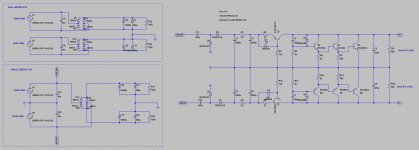
You can connect to the AC output that goes to BR's.
The thing is to connect positive side to the BR on positive side or you will get negative voltage because it's connected on "wrong side" of ground.
Figge
The thing is to connect positive side to the BR on positive side or you will get negative voltage because it's connected on "wrong side" of ground.
Figge
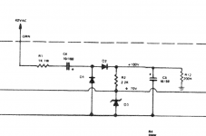
IPS bias voltage.
This is from the Crown DC300A schematic.
Some important points are:
1. C4 must be a SMALL capacitor in order to limit the current and therefore not waste a lot of power and heat.
2. D3 is a 10 Volt Zener tied from +60 to +70. This circuit adds 10V to the main 60V rail. It does not return to ground.
Be mindful that a high current supply is a huge waste. Estimate the IPS current draw and shunt no more than 2x that current. The shunt current in D3 is all that's needed and there is no added transistors. The problem is that while a voltage doubler allows stacking voltage on top of the main supply, it naturally generates too much voltage so you have to drop that voltage with a small capacitor in the AC and resistors in the DC. Note that if the doubler is overloaded, D3 becomes forward biased and the IPS voltage drops no lower than the main supply. Also note that a 10V Zener produces a lot less heat than a 50V - 70V shunt.
A more efficient circuit uses a ~3 Henry inductor in place of D1. That would make the circuit a half wave rectifier without voltage doubling. But, of course, large inductors are avoided when ever possible.
Attachments
Hi,
The LEDs is very sensitive with temperature. You need to consider using it in CCSs. The thermal drift may change your currents. I only use LEDs in voltage references for cascode where the change of LED Vf does not affect significantly.
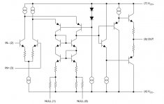
// I usually see folded cascode topology in hi speed voltage feedback op-amps, but not same as your.
The LEDs is very sensitive with temperature. You need to consider using it in CCSs. The thermal drift may change your currents. I only use LEDs in voltage references for cascode where the change of LED Vf does not affect significantly.
// I usually see folded cascode topology in hi speed voltage feedback op-amps, but not same as your.
Attachments
- Home
- Amplifiers
- Solid State
- Folded cascode lateral MOSFET power amp