I am fond of the lateral mosfet OPS power amps and after building two successful examples:
Assemblage Power Amp
and the bigger lin type:
Very HQ power amplifier (Assemblage VII)
I want to build another one with hopefully even better high frequency response.
Recently read this paper by Bob Cordell http://www.cordellaudio.com/JFETs/LSK489appnote.pdf
where I found a DOPA using a folded cascode IPS and decided this would be a good start for my new power amp.
Allready simulated one possibility but have some doubts about it's viability.
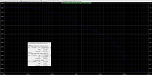
My sim indicates this design is stable even without compensation.....
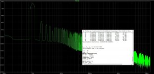
I can not reduce 1khz distortion below 0.015% THD....
I am not sure about the best ccs to use for the folded cascode IPS....
Hope my design captures enough interest and discussion so I can improve this solution.
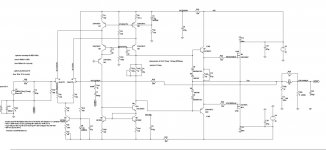
Please find the schematic and asc file in attach
Best
Ricardo
Assemblage Power Amp
and the bigger lin type:
Very HQ power amplifier (Assemblage VII)
I want to build another one with hopefully even better high frequency response.
Recently read this paper by Bob Cordell http://www.cordellaudio.com/JFETs/LSK489appnote.pdf
where I found a DOPA using a folded cascode IPS and decided this would be a good start for my new power amp.
Allready simulated one possibility but have some doubts about it's viability.
My sim indicates this design is stable even without compensation.....
I can not reduce 1khz distortion below 0.015% THD....
I am not sure about the best ccs to use for the folded cascode IPS....
Hope my design captures enough interest and discussion so I can improve this solution.
Please find the schematic and asc file in attach
Best
Ricardo
Attachments
Last edited:
Should tha folded cascodes Q5 and Q6 perhaps have a stiffer voltage source foe bias? Maybe just some cap to gnd, in parallel with R32.
The 2pF you have there...are they to sim parasitics or are you actually having those in the ckt?
Sorry I am not answering your question but giving you some instead.
The 2pF you have there...are they to sim parasitics or are you actually having those in the ckt?
Sorry I am not answering your question but giving you some instead.
Hi
Welcome to the fan club of the lateral mosfet 😛
This reminds me of the FC-100 front stage but you have replaced the bjt ou out stage with lateral mosfet. I had also thought about that after I saw the FC-100...
RMI-FC100, a single stage audio power amplifier
This should be interesting 🙂
Input impedance should be easily more than 22k with jfet as input.
Protection diodes orientations seem backward.
C1 and C2 has a negligible effect with so low value.
Q5 and Q6 could have base resistors to prevent possible oscillation.
What IDSS of input jfet ?
Fab
Last edited:
Should tha folded cascodes Q5 and Q6 perhaps have a stiffer voltage source foe bias? Maybe just some cap to gnd, in parallel with R32.
The 2pF you have there...are they to sim parasitics or are you actually having those in the ckt?
Sorry I am not answering your question but giving you some instead.
Hi semperfi
I experienced oscillations in one of my builds that used a cap over r32 so I did not include it here.
The 2p caps are there for sim purposes only... they are not effective with so low values but if I increase them to 47p I have phase margin of 70...
Hi fabHi
Welcome to the fan club of the lateral mosfet 😛
This reminds me of the FC-100 front stage but you have replaced the bjt ou out stage with lateral mosfet. I had also thought about that after I saw the FC-100...
RMI-FC100, a single stage audio power amplifier
This should be interesting 🙂
Input impedance should be easily more than 22k with jfet as input.
Protection diodes orientations seem backward.
C1 and C2 has a negligible effect with so low value.
Q5 and Q6 could have base resistors to prevent possible oscillation.
What IDSS of input jfet ?
Fab
Thank you for the link... will study it...
Will place base stoppers in at q5 q6 as suggested
Will also increase input impedance...
The flying catch diodes are ok... I am using the same ops in other builds....
The ips runs at 4ma..
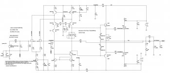
The folded cascode provides a current gain of 1A/1A, i.e. unity. Thus forward transconductance is given by the JFET differential pair and this is restricted by the source degeneration of 100R to <10mA/V. From that point of view the loop gain is somewhere in the middle of the road and resulting in good, but not exceptional THD.Mods included... please comment...
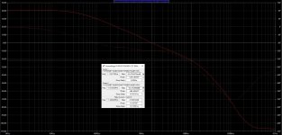
You should simulate the open loop gain with LTSpice to investigate possible improvements.
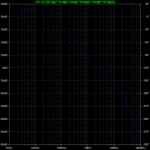
TIAN shows results without any compensation...... Is it possible this type of IPS does not need compensation ?
Too small gain, folded cascode could be a way better in terms of gain.
Just a few comments regarding improvements. Pointing to schematic on post 8:
- Make sure IC_Q1 and IC_Q2 are more than 2x IC_Q3 in quiescent conditions. Else, when amp is slewing, IC_Q5 or IC_Q6 will go to 0 and recovery is terrible.
- Replace R4 with a diode (3 diode string or 2 Green LEDS like D1). See the schematic for the RMI-FC100.
- Connect C3 to the positive supply not ground. The bias voltage of Q5 and Q6 base is referenced to the positive supply, else PSRR+ will be mediocre. Think of it this way. If VCC moves and the base of Q5 and Q6 does not, the VCE of Q1 and Q2 get modulated. Their currents will change, and mismatches will give you bad PSRR+.
- Tie the base of Q4 to the emitter of Q7. This way, both sides of the Folded cascode are modulated with output swing. This will boost your open loop gain.
- I would put compensation caps to ground on the bases of Q7 and Q10. Currently all your compensation is CJC of Q6, Q7, Q10, Q11. This has 2 problems:
1. It is unpredictable due to component variation. You just don't know what you will get from the factory, so your amp's unity gain frequency (UGF) will be anyone's guess.
2. CJC is non-linear, hence your THD won't be particularly great. On this point, this is one of the Achilles heels of single stage power amps. If you want to go crazy, you can bootstrap CJC Q7 and Q10. Driving Q4 base will eliminate Q6 CJC within the mismatch of Q6 and Q5 CJC. Eliminating CJC Q11 is more difficult, you would need to a fancy current mirror like the AD797, but I don't advise it.
Hope it helps, Sandro
Last edited:
Interesting Amp but there a couple issues that the RMI-FC100 has already solved.
1. Drivers operates from the same 43VDC as the outputs which means clipping is about 33V, ie about 3/4 of the main supply and about half the potential power output.
2. The 2SK170 JFETs are rated 40VDC which limits the driver voltage. The RMI-FC100 adds another cascode stage to take voltage off these JFETS. A simpler alternative might be to add (bypassed?) dropping resistors on the JFET drains.
Thanks for posting something interesting. Too many posts about choosing ridiculously expensive caps and transformers for building dinosaur amps and people who don't understand basic bias drops.
I should also mention that my simulation keep telling me that asymmetric VAS works better than symmetric circuits, assuming it operates class A, a little counter intuitive.
And defining the VAS operating current of asymmetric VAS is way easier, and also easy to get better voltage swing. For BJT, 3EF may be a better investment, probably not for MOSFETs.
Hi Steveu, can you expand on: "I should also mention that my simulation keep telling me that asymmetric VAS works better than symmetric circuits, assuming it operates class A, a little counter intuitive.
And defining the VAS operating current of asymmetric VAS is way easier, and also easy to get better voltage swing. For BJT, 3EF may be a better investment, probably not for MOSFETs."
Also, there is no VAS in this design. This is a single stage amplifier.
Best, Sandro
And defining the VAS operating current of asymmetric VAS is way easier, and also easy to get better voltage swing. For BJT, 3EF may be a better investment, probably not for MOSFETs."
Also, there is no VAS in this design. This is a single stage amplifier.
Best, Sandro
Try something like attached.
First of - inverting. This will eliminate common mode error from the input stage.
Second - doesn't forget about VAS output loadind, dropping this will result in hardly to find leaks from fingerprints on the board.
Third - add filters for voltage sources.
Last - too much voltage loss in the VAS stage. It's better to provide different lower supply to the MOSFETs.
Attachments
Last edited:
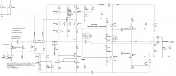
After some experimentation and following some of your ideas I made some adjustments:
LSK489 in the IPS because matched device with 60V breakdown voltage (in the FC-100 I see roender used a cascode that lowers voltage over the k170 but I am not sure it helps in my case... please comment)
Added c1 c2 10p from Q6 Q11 collectors to gnd to be sure the amp is stable without depending on internal bjt capacitances (this comes from roender design also).
Reduced ips jfet source resistors and increased tail current to 4.3mA ( being sure Q1 Q2 current is higher than double tail current)
Did not drive Q4 as suggested because that increases THD.
Using only two laterals on the output I believe I can leave the drivers Q7 Q10 current at 25mA.
Attachments
Try something like attached.
First of - inverting. This will eliminate common mode error from the input stage.
Second - doesn't forget about VAS output loadind, dropping this will result in hardly to find leaks from fingerprints on the board.
Third - add filters for voltage sources.
Last - too much voltage loss in the VAS stage. It's better to provide different lower supply to the MOSFETs.
Thank you so much
I find your solution very interesting principally due to the fact we eliminate common mode error from ips.
I know I should have higher rails in the input stage but I feel using only one psu is simpler to build.
Interesting Amp but there a couple issues that the RMI-FC100 has already solved.
1. Drivers operates from the same 43VDC as the outputs which means clipping is about 33V, ie about 3/4 of the main supply and about half the potential power output.
2. The 2SK170 JFETs are rated 40VDC which limits the driver voltage. The RMI-FC100 adds another cascode stage to take voltage off these JFETS. A simpler alternative might be to add (bypassed?) dropping resistors on the JFET drains.
Thanks for posting something interesting. Too many posts about choosing ridiculously expensive caps and transformers for building dinosaur amps and people who don't understand basic bias drops.
I should also mention that my simulation keep telling me that asymmetric VAS works better than symmetric circuits, assuming it operates class A, a little counter intuitive.
And defining the VAS operating current of asymmetric VAS is way easier, and also easy to get better voltage swing. For BJT, 3EF may be a better investment, probably not for MOSFETs.
I plan to use LSK489 dual fets on the input.... as these sport higher breakdown voltage (60V) maybe I can get away without the cascode.... or do you believe this additional cascode is somehow beneficial to the amp response ?
I simulated the amp with the additional cascode and THD is not as good ... please comment.
Attachments
LSK489 in the IPS because matched device with 60V breakdown voltage (in the FC-100 I see roender used a cascode that lowers voltage over the k170 but I am not sure it helps in my case... please comment
Keep jfets current as high as possible due to that's the all available current to drive VAS output node.
But that case you need to keep dissipation in safe margins and cascode are great help.
I know I should have higher rails in the input stage but I feel using only one psu is simpler to build.
But having so high rails at the OPS devices will greatly impact on SOA. If you could estimate dissipation on the nonresistive load such a speaker - you'll find a need of more robust OPS devices.
- Home
- Amplifiers
- Solid State
- Folded cascode lateral MOSFET power amp