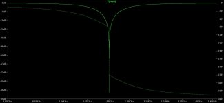
-92dB simulated notch with the AD8397 and +/-12Vdc
Here is an interesting discovery on this project.
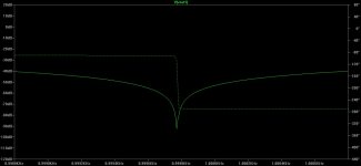
The AD8397 results in a simulated notch at -92dB vs -72dB with the THS4031. The part is only 26V max, so the power supplies are reduced to +/-12Vdc. It is unity gain stable but the bandwidth is nowhere near 100MHz. 69Mhz for extremely small signals. The phase transition at the notch frequency appears to simulate as being much sharper than the THS4031/2.
This is a dual chip, so it wouldn't mount since the board requires 2 single chips. Just interesting results.
Here is an interesting discovery on this project.
The AD8397 results in a simulated notch at -92dB vs -72dB with the THS4031. The part is only 26V max, so the power supplies are reduced to +/-12Vdc. It is unity gain stable but the bandwidth is nowhere near 100MHz. 69Mhz for extremely small signals. The phase transition at the notch frequency appears to simulate as being much sharper than the THS4031/2.
This is a dual chip, so it wouldn't mount since the board requires 2 single chips. Just interesting results.
Attachments

Last edited:
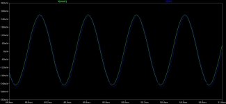
I ran out of edit time on the post above. I completely forgot about the frequency-adjust trimpot on the board.🙂 About 20 degrees of clockwise rotation (I centered that 25-turn pot before solding it in) it appears to have completely zeroed out the 5mV p-p output I was seeing at 1.0000KHz. So apparently the notch is even deeper than -40dB. Going up to 2mV sensitivity on the scope there is so much noise, without being in a shielded box, that I really can't extract anything useful in terms of notch output although it "looks" flat. So at this point I can't say what the actual notch depth is, other than "greater than -40dB"
Time to hook up the QA400. 🙂
Speaking of shielded boxes, this board would fit inside the same Hammond 1598REBK case I used for the Victor oscillator board power supply project I have posted in another thread. That case can take a roughly 140 x 140mm board. This one is 130 x 120. I have 3mm mounting holes at the corners of this one that will fit M3 nylon standoffs. I don't have holes in this one to match up with the 4 mounting studs molded in the bottom of that case, so you would have to drill 4 mounting holes up through the bottom of the case.
Nice work.
But as I remember, I've build this notch filter before. The notch depth is good, but the THD seems not acceptable, only ~-90dB to -100dB in my bench.
marce - my attempt at reducing the chances of input-to-output capacitive coupling, especially since the original try (with the LME49990s) oscillated. Probably an over-reaction. 🙂 Hey I know from your posts that you have done a huge amount of PCB layout. What would you suggest here, leaving the ground plane everywhere? The oscillation problem was solved by going to the THS4031. Input-output coupling probably wasn't the issue.
bbp - interesting! Which chip did you use, the THS4031/2? If so I was kind of expecting that (high(er) THD) based on the THS4031/4032 datasheet specs. That is why I tried the LME49990 in the first place, extremely low THD, along with being a 110MHz chip. The LME49990 *should* be the perfect chip for this thing, on paper at least, if it wasn't for the oscillation problem.
In fact, more I think about it, now that I have the board working and "proved" (with the THS4031), I think that I'm going to go back and swap in LME49990s one at a time. Maybe it is just one of the two op-amp positions that are having the oscillation problem. I'm also going to try adding that exact RLC network that National lists in the datasheet: 33R + 270nH + 10pF (the section of the datasheet below). Lets see if that "fixes" it. 🙂
I realized yesterday the solution to the S/N problem of "seeing" the bottom of the notch through the noise on the scope is already on the board! Lol, I completely forgot about the post-filter-amplifier I have at the top. I'll set it up for 5x voltage gain to start and run the notch filter output through it. That should bump the 5mV peak up to 25mV peak. The extra amp will add some noise, of course, but at least it will let me calculate notch depth.
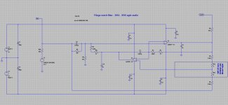
The AD8397 simulation has me intrigued enough to consider sending in a dual-chip version of the notch filter for fab, intial layout below. Presumably this layout would work for the THS4032 dual chip version too. I've stripped out all the alternative package sizes and types for the frequency "set" resistors and capacitors, just 0805 SMD throughout to shrink it down a bit. The adjustable voltage regulators would be set for the +/-12Vdc. I've added parallel tantulum bypass caps to the BUF634. My first attempt at adding them to the filter chip made things a bit too large. I'm going to try again. I'm planning on using those new 4.7uF 35V X7R MLCC's for the ceramic bypass, so I'll probably use 47uF solid tantalums. I've added a position for the 49.9R input-to-ground resistor now.
I realized this morning why I happened to have the AD8397 model already added to LTSpice in the first place. That is the chip AMB uses in his mini^3 headamp. As I recall the design history of that project, from reading through the old posts on Headwize once, the chip had oscillation problems which is how the 6R or so wound up in series with the output (inside the headamp's feedback loop). Seems that I recall posts from Tangent and folks during that era indicating they were all having oscillation troubles in trying to use the chip. This will be interesting.
bbp - interesting! Which chip did you use, the THS4031/2? If so I was kind of expecting that (high(er) THD) based on the THS4031/4032 datasheet specs. That is why I tried the LME49990 in the first place, extremely low THD, along with being a 110MHz chip. The LME49990 *should* be the perfect chip for this thing, on paper at least, if it wasn't for the oscillation problem.
In fact, more I think about it, now that I have the board working and "proved" (with the THS4031), I think that I'm going to go back and swap in LME49990s one at a time. Maybe it is just one of the two op-amp positions that are having the oscillation problem. I'm also going to try adding that exact RLC network that National lists in the datasheet: 33R + 270nH + 10pF (the section of the datasheet below). Lets see if that "fixes" it. 🙂
I realized yesterday the solution to the S/N problem of "seeing" the bottom of the notch through the noise on the scope is already on the board! Lol, I completely forgot about the post-filter-amplifier I have at the top. I'll set it up for 5x voltage gain to start and run the notch filter output through it. That should bump the 5mV peak up to 25mV peak. The extra amp will add some noise, of course, but at least it will let me calculate notch depth.
The AD8397 simulation has me intrigued enough to consider sending in a dual-chip version of the notch filter for fab, intial layout below. Presumably this layout would work for the THS4032 dual chip version too. I've stripped out all the alternative package sizes and types for the frequency "set" resistors and capacitors, just 0805 SMD throughout to shrink it down a bit. The adjustable voltage regulators would be set for the +/-12Vdc. I've added parallel tantulum bypass caps to the BUF634. My first attempt at adding them to the filter chip made things a bit too large. I'm going to try again. I'm planning on using those new 4.7uF 35V X7R MLCC's for the ceramic bypass, so I'll probably use 47uF solid tantalums. I've added a position for the 49.9R input-to-ground resistor now.
I realized this morning why I happened to have the AD8397 model already added to LTSpice in the first place. That is the chip AMB uses in his mini^3 headamp. As I recall the design history of that project, from reading through the old posts on Headwize once, the chip had oscillation problems which is how the 6R or so wound up in series with the output (inside the headamp's feedback loop). Seems that I recall posts from Tangent and folks during that era indicating they were all having oscillation troubles in trying to use the chip. This will be interesting.
Attachments

Last edited:
I'm not marce but ...marce - my attempt at reducing the chances of input-to-output capacitive coupling, especially since the original try (with the LME49990s) oscillated. Probably an over-reaction. 🙂 Hey I know from your posts that you have done a huge amount of PCB layout. What would you suggest here, leaving the ground plane everywhere?
Think about where the return current will flow and keep the loop small.
marce - my attempt at reducing the chances of input-to-output capacitive coupling, especially since the original try (with the LME49990s) oscillated. Probably an over-reaction. 🙂 Hey I know from your posts that you have done a huge amount of PCB layout. What would you suggest here, leaving the ground plane everywhere? The oscillation problem was solved by going to the THS4031. Input-output coupling probably wasn't the issue.
bbp - interesting! Which chip did you use, the THS4031/2? If so I was kind of expecting that (high(er) THD) based on the THS4031/4032 datasheet specs. That is why I tried the LME49990 in the first place, extremely low THD, along with being a 110MHz chip. The LME49990 *should* be the perfect chip for this thing, on paper at least, if it wasn't for the oscillation problem.
In fact, more I think about it, now that I have the board working and "proved" (with the THS4031), I think that I'm going to go back and swap in LME49990s one at a time. Maybe it is just one of the two op-amp positions that are having the oscillation problem. I'm also going to try adding that exact RLC network that National lists in the datasheet: 33R + 270nH + 10pF (the section of the datasheet below). Lets see if that "fixes" it. 🙂
I realized yesterday the solution to the S/N problem of "seeing" the bottom of the notch through the noise on the scope is already on the board! Lol, I completely forgot about the post-filter-amplifier I have at the top. I'll set it up for 5x voltage gain to start and run the notch filter output through it. That should bump the 5mV peak up to 25mV peak. The extra amp will add some noise, of course, but at least it will let me calculate notch depth.
The AD8397 simulation has me intrigued enough to consider sending in a dual-chip version of the notch filter for fab, intial layout below. Presumably this layout would work for the THS4032 dual chip version too. I've stripped out all the alternative package sizes and types for the frequency "set" resistors and capacitors, just 0805 SMD throughout to shrink it down a bit. The adjustable voltage regulators would be set for the +/-12Vdc. I've added parallel tantulum bypass caps to the BUF634. My first attempt at adding them to the filter chip made things a bit too large. I'm going to try again. I'm planning on using those new 4.7uF 35V X7R MLCC's for the ceramic bypass, so I'll probably use 47uF solid tantalums. I've added a position for the 49.9R input-to-ground resistor now.
I realized this morning why I happened to have the AD8397 model already added to LTSpice in the first place. That is the chip AMB uses in his mini^3 headamp. As I recall the design history of that project, from reading through the old posts on Headwize once, the chip had oscillation problems which is how the 6R or so wound up in series with the output (inside the headamp's feedback loop). Seems that I recall posts from Tangent and folks during that era indicating they were all having oscillation troubles in trying to use the chip. This will be interesting.
I am going to look at the chips and schematic more this weekend, but apart from some very high speed ADC's (where the ground is cut from under the input pins) I always use a contiguous unbroken ground plane. I've read some of the stuff you have posted and will look further at it this weekend, in a hotel and working on site so have limited internet access during the week at the moment.
I think a board respin would kindle my desire to build one of these, especially if it fit in the Hammond enclosure directly 🙂
marce - thank you! Any input is appreciated.
hochopeper - I agree. One thought here is to reduce to the cut-outs (back) to just directly under the chips. I've done that on a few other posted projects here and its has worked out well. I've also seen mention of that in a few datasheets over the years, removing the planes directly under the chips to help reduce the input-to-ouptut cap coupling.
luvdunhill - I think I may do that, make it fit the 1598REBK case. I have an idea there, too. I might try to fit two copies of the notch filter and BNCs on the expanded board (two channels). I was looking at the dimensions a couple of days ago. The board would become 10mm wider and 20mm longer. That extra length may be enough to move the post-filter-amplifier section out from between the BNCs to between the notch filter and BNCs. Then I could pop another channel in the extra space. For single channel use just don't populate the parts on one of the notch filters. With two channels I should be able to get 1KHz and 10KHz notches at the same time, or 10KHz and 11KHZ for IMD, unless there is some interaction between the channels through the power supply. Going from 1KHz to 10KHz on the board is easy. Just replace the two 0.047uF with 0.0047uF. I have a part number for one of those (1%, C0G MLCC, 0805 size) in the BOM I'm putting together, as an alternate part.
I kind of like that particular case in that it comes in the cheaper non-shielded version along with the shielded.
Last edited:
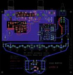
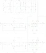
A dual Fliege notch filter PCB for the Hammond 1598EBK series case
Here is a rough-in of two Fliege notch filters on a PCB that fits the Hammond 1598EBK/1598REBK series case. They do fit!
I've moved the post-filter-amplifier from between the BNCs to below each notch filter circuit. This board is the exact size for the 1598EBK case series, complete with side notches and the four 3.5mm holes for truss head screws into the case mounting bosses. Much layout & schematic clean-up yet to be done through.
Attachments


Last edited:
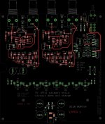
Back home so I will look in more detail. Again I would not cut the ghrtound plane from under any devices, it is not necessary and is bad practice DONT DO IT. Sorry to get loud but it is critical especially around high speed op-amps and for the best signal integrity (at all frequencies). I have more comments but rather than put them in words I am going to copy one channel to illustrate the points I want to make, so give us a couple of hours (Friday and Saturday are my weekend when I am working on customers site, drive down Sunday and do 4 10+ hour days).
From a drafting point of view your schematic is spread out a tad to much, it also looks like a BOM and schematic joined together in unholy matrimony, use a BOM for all the relevant component information, on a schematic limit this to values, voltage, etc. things that are pertinent when using a schematic.
🙂
Hi.
Is it ok to use the same groundplane between the filters? No crosstalk?
Regards
Yes, don't start splitting ground planes it is probably one of the worse things you can do to a low level design. When I get chance I have a whole library of documentation from all your favourite IC companies and others on low level high resolution design practices.
On the M3 mounting holes add a 7mm diameter land top and bottom, this is the size of a washer or nut with a bit of a safety margin, then you wont short copper or traces out by accident if you get them too near.
I won't 🙂 as I take your word for it. I was merely thinking that this is to different circuits sharing the same groundplane and that might have some complications. But I'll believe you if you say it would worsen things.
Regards
Regards
Yes, don't start splitting ground planes it is probably one of the worse things you can do to a low level design. When I get chance I have a whole library of documentation from all your favourite IC companies and others on low level high resolution design practices.
On the M3 mounting holes add a 7mm diameter land top and bottom, this is the size of a washer or nut with a bit of a safety margin, then you wont short copper or traces out by accident if you get them too near.
When I get chance I dig out the relevant stuff.
For a real illustration the librarys, base schematic and board I have just stripped all the stuff of to re-create the notch filter on had about 62 8 leg op-amps (mostly OP249GS) in numerous channels for the analogue interface to sensors etc. for control of a critical bit of equipment, the only split in the grounds was between the digital ( logic, processor, communications) and the above analogue section and the chassis (Case, what would be directly fastened to PE in domestic gear). No problems with any channel cross talk (Board is 475mm X 275mm 6 Layers). My preference for true isolation would be a real double mono design, but even here there will be some channel coupling somewhere in the total set up (everything that is plugged in) and often that coupling can be a major irritation (ground loops, we all know and love them). So trying to isolate on a low level design can cause more issues because you may create a coupling mechanism that is far more problematic than two circuits on the same ground plane. Keep the circuitry apart, and lay out as dual mono's and lay them out so that from input to output no signals cross. There are a few things and options, let me do one channel first then I can copy that and we can visually look at the various methods used throughout the analogue fraternity (all analogue fast slow etc) and also discuss why some things are important for EMC (especially RF) and signal integrity.
For a real illustration the librarys, base schematic and board I have just stripped all the stuff of to re-create the notch filter on had about 62 8 leg op-amps (mostly OP249GS) in numerous channels for the analogue interface to sensors etc. for control of a critical bit of equipment, the only split in the grounds was between the digital ( logic, processor, communications) and the above analogue section and the chassis (Case, what would be directly fastened to PE in domestic gear). No problems with any channel cross talk (Board is 475mm X 275mm 6 Layers). My preference for true isolation would be a real double mono design, but even here there will be some channel coupling somewhere in the total set up (everything that is plugged in) and often that coupling can be a major irritation (ground loops, we all know and love them). So trying to isolate on a low level design can cause more issues because you may create a coupling mechanism that is far more problematic than two circuits on the same ground plane. Keep the circuitry apart, and lay out as dual mono's and lay them out so that from input to output no signals cross. There are a few things and options, let me do one channel first then I can copy that and we can visually look at the various methods used throughout the analogue fraternity (all analogue fast slow etc) and also discuss why some things are important for EMC (especially RF) and signal integrity.
I love analogue layout far more than digital and tend to do more and more of it these days, mentally its more taxing and much more fun debating circuitry with analogue engineers, they do have often quite different views and debates can be interesting. Once you get high speed digital rules into your head the rest becomes easy (well after a few hundred designs, but a DDR memory interface is a DDR memory interface) whereas analogue can vary from DC to GHz all with there own problems and similarly with voltage and current levels, also audio, instrumentation control etc.
Marce, I envy you if you have this as an profession. I started a long time ago with home electronics followed by radio transmission circuits for a to short period. Then it has been computers and their needs all the way. Maybe I were more fit to decipher two states - 0 and 1 but my feeling does not allways agree with what is practical. Well its agdr's circuit and I'm a meere follower and interested in a few boards further on.
Regards
Regards
I've done PCB layout for 30+ years now🙂
Anyway a chick channel layout, doing the schematic was a pain!!! Layout was fun.
LNK1 and 3 are the input connectors, didn't have time to do a proper part.
Back soon got to play taxi driver for the missis.
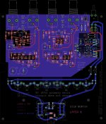
Schematic attached as well.
Anyway a chick channel layout, doing the schematic was a pain!!! Layout was fun.
LNK1 and 3 are the input connectors, didn't have time to do a proper part.
Back soon got to play taxi driver for the missis.
Schematic attached as well.
Attachments
marce - WOW! 🙂 I certainly appreciate your time and effort here. Very very helpful.
I'll take your suggestion and eliminate the cut-outs under the chips. I would trust years of experience over a couple of random datasheet comments any day! That will save a bunch of layout time too. Takes quite a while to get cut-outs for 3 layers lined up in Eagle.
Your discussion with Turbon has probably just prevented a mistake I was about to make. 😀 On the double-channel version posted above I had been playing around with the idea of making two copies of the voltage regulators, one for each of the channels, moved to the bottom between the batteries and the post-filter-amplifiers. Then splitting the ground plane in the middle between the channels, about 80% of the way down.
But marce you make an excellent point about ground loops here. If I split most of the that ground plane between the channels, it will simply get re-connected again at the BNC end. Worse still, these BNC housings are plastic so the grounds wouldn't re-connect at the front panel, they would re-connect inches away at the scope or wherever the BNC cables from the two channels meet up again. So back to just keeping the existing single power supply for the whole thing.
I agree with your comments about dual-mono 100%. To really make that work the power supplies & their grounds need to be electrically isolated too, i.e. what is feeding the voltage regulators (two transformers, or separate isolated windings). Then there would be no chance of front-end connections forming a ground loop.
I agree about a split between any digital and analog ground planes probably being the one big technically justified split.
Lol, good comments about the part spacing and part numbers on the schematic. 🙂 The wider spacing I've done to help make it easier for folks to DIY hand-solder, but I agree that I've over done it. If it was going to be wave soldered I would definitely shrink it way down.
The part numbers on the schematic is a recent thing I started doing. I've found that when I design these things I typically go search for what's available at Mouser during the schematic stage, then forget which part I saw when it came time to put the BOM together and have to go back through the Mouser listings. 😛 So putting the part numbers on there helps assemble the BOM at the end faster. I agree though it does clutter things up. The part numbers tend to be long. Plus there is the problem about a part going out of stock or becoming obsolete - and now it is on the schematic forever. What I'll do here is delete those part numbers once I get the BOM finalized. Thanks again for the comment!
I'll study your layout! I can see a lot of helpful technique already. One question right up front is vias - and traces for that matter - under the ICs. So far I've avoided vias under chips, but I see you have used one. I guess my concern has been the IC laying flat for soldering (in the case of the via) and proximity capacitive coupling between traces in the case of traces under there. I'll bet traces under the chips is one of those frequency-sensitive things. For the frequencies involved here it probably doesn't matter.
Same with grounding the bypass caps, I see you've used a single via. That must be adequate, at least at these fairly low frequenices.
Thank you again!!
Last edited:
Its easier to illustrate graphical things with pictures than try and put it into words🙂
Layout is 90% placement 10% routing from a skills point of view. If you have connections that rubber band when you are doing the placement look at the patterns that you create as you move the components, picturing the routes from the connectivity. The best way of learning this is trying one placement, routing it, trying another until you get the best result. There are rules that are defined by the devices function and the schematic, the schematic being your map of electrical connectivity. That is why I drew the schematic in what is almost a classic style, feedback loops are drawn clearly and stand out more, decoupling is clearly shown and signal references are used for power connections to minimise the connections that have to be followed.
So when you are laying out analogue sections, break the circuit down...
Start with input and output connectors, so you can determine the circuits flow from input to output. Then for the individual op-amps build up an initial block, place the decoupling caps first, second feedback loops and input resistors. When you have built you initial circuit blocks you can then move them about and again see the interactions of connections as you place the blocks. Eventually you'll have built up your complete circuit.
Doing a board this way is the best method, concentrate on getting neat basic circuitry blocks, usually an op-amp gate or several, minimising loop areas, especially when using high speed op-amps, then concentrate on putting the blocks together like a jigsaw, again going for optimum connection patterns between blocks.
Where you have sections that operate on different supplies, try and group the ICs and components referenced to a certain voltage in the same area. This is more critical with high speed digital as the signal is referenced to both positive and the 0V supply so both return paths should be considered; running critical signals between a contiguous GND plane and a positive supply plane seem to be the best option for ultimate signal.
Finally treat it as a challenging game and enjoy it. If a bit of layout is frustrating you, do another area or relax, then look at it again later.
No we don't worry about vis under IC's on many designs the lack of room dictates any available space is utilised. For very high speed analogue the rules do change a bit, but here we are going to be in the high MHz's low GHz's.
Having separate power supplies, but the same ground is an often used technique and may be worth considering. A main supply is provided round the periphery of the board (where possible, as bus bar routing (broadside coupled)) to local well filtered supplies for each section (the same 0Vs though) this has numerous benefits, the overall circuitry is better confined to a well defined area with decoupling caps and the local supply forming a localised power loop and crosstalk between the sections is reduced especially any noise the circuitry adds to the supplies.
Decoupling caps I must admit I was a bit tardy with and rushed the layout (otherwise I would have had no time, busy weekend and in a hotel Sun-Fri) and where possible prefer at least two vias either side of the cap and towards the centre of the device to minimise loop area, again low frequency is much more forgiving than high frequencies (here planar capacitance would be my first line of decoupling followed by small local decouplers (0402's or smaller).
I did think the spacing was for DIY, but people can DIY when the components are closer, better to develop the assembly skills than compromise the design in my view.🙂
- Home
- Design & Build
- Equipment & Tools
- Fliege 1kHz notch filter project PCB