Hvala ti very much aparatusonitus. I am very glad to know that you are from Split, where my grandparents were born. I am old now but I still remember such beautiful stories from that place. I am honoured.
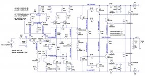
First off all I will apologize because I made a serious mistake when uploading the original circuit. Two transistors Q7 and Q14 were missing and here is the corrected version. I spend a lot of time to figure the circuit out and I will still be checking again today. Please excuse me, I never had an original schematic.
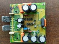
This is how these 2 amplifiers worked fine for +10 years, knowing that they have plenty of design errors. These are the original values installed on the boards. And this in one of my problems, because I can't make the copies work.
The simulation throw awful results in frequency response being original 100pF C17 and C8 guilty. Strange that the previous simulation worked as well.
It is very interesting this new transistors data you provided. I will order the parts from Mouser. However this will take about 6 days to arrive in. I think we can still experiment with the old ones and test to see if the oscillation stops. As I said, I made it stop with C3 and C4 100pF but for some reason the MOSFETs get very hot.
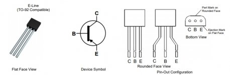
Yes, 2N5401/5551 and ZTX656/756_ZTX657/757_ZTX658/758 have the same pin orientation, 180° rotated from BC546/BC556.
I understand what you say about unmounting MOSFETs and testing without them. I don't want to play foolish but if I make shorts tests, these small VAS transistors get hot but can withstand the test until I can get some values and check if there is some other coarse error on the board, until I bring the new Zetex transistors. What do you think ?
First off all I will apologize because I made a serious mistake when uploading the original circuit. Two transistors Q7 and Q14 were missing and here is the corrected version. I spend a lot of time to figure the circuit out and I will still be checking again today. Please excuse me, I never had an original schematic.
This is how these 2 amplifiers worked fine for +10 years, knowing that they have plenty of design errors. These are the original values installed on the boards. And this in one of my problems, because I can't make the copies work.
The simulation throw awful results in frequency response being original 100pF C17 and C8 guilty. Strange that the previous simulation worked as well.
It is very interesting this new transistors data you provided. I will order the parts from Mouser. However this will take about 6 days to arrive in. I think we can still experiment with the old ones and test to see if the oscillation stops. As I said, I made it stop with C3 and C4 100pF but for some reason the MOSFETs get very hot.
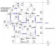
Therefore, if 2N5401/5551 were used on the second differential, you would have to rotate the Zetex transistors by 180°.
Yes, 2N5401/5551 and ZTX656/756_ZTX657/757_ZTX658/758 have the same pin orientation, 180° rotated from BC546/BC556.
I understand what you say about unmounting MOSFETs and testing without them. I don't want to play foolish but if I make shorts tests, these small VAS transistors get hot but can withstand the test until I can get some values and check if there is some other coarse error on the board, until I bring the new Zetex transistors. What do you think ?
Attachments

With disassembled power MOSFETs there is a substantial risk to burn the drivers. And it is mandatory to remove any load as well, an output short will definitely end in fireworks.
I suspect without the power MOSFETs oscillations will vanish - so removing them is not really helpful.
In your case I would mount the power MOSFETS and the 100pF to tame oscillations.
Adjust output bias to 100mA total.
And then proceed with troubleshooting oscillations.
I suspect without the power MOSFETs oscillations will vanish - so removing them is not really helpful.
In your case I would mount the power MOSFETS and the 100pF to tame oscillations.
Adjust output bias to 100mA total.
And then proceed with troubleshooting oscillations.
Hello voltwide, understood. I will take the risk using the ruined original board that still has all its components mounted except for the blown MOSFETs.
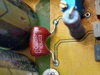
As additional info, with C3 and C4 = 100pF (huge value) oscillations stop and as I said MOSFETs get hot in no more than 6 seconds in which I cut power (I am using a variac very carefully). As I explained before, at that point all 4 gates receive a very large voltage of more than +/-6V when the simulation shows about +/-430mV with the input grounded. In this condition the MOSFETs bias current is ~500mA !!!! I have cut a trace and inserted a 0.1 Ohm 3W 1% wire wound resistor (picture) to measure this quiescent current that as you said before should be in the order of 100mA. My last version of a simpler similar amplifier (almost same circuit) had 130 mA bias.
This is why I have reached a point in which I need to isolate something to check what is raising this gate voltages so much. With this high gate voltages it is logical that the MOSFETs are running in the active region to the point to short the power supply. Do you agree ?
Attachments
What's the voltage across R7 - that should be the bias setting - the various driver emitter voltages step down from that, so Q7 to Q14 emitter voltage should be less, and Q4 -- Q13 emitter voltage span even less. The gate-to-gate voltage on the output devices should be the same as this last.
Hello Mark Tillotson, a quick test of 1 second at full power supply shows 14V ! MOSFETs are hot.
Hvala ti very much aparatusonitus. I am very glad to know that you are from Split, where my grandparents were born. I am old now but I still remember such beautiful stories from that place. I am honoured.
Glad to meet someone on the other side of the world especially since your roots are from Split. And make sure the stories your parents told you about living in Split are true...it was like living in one of the Federico Fellini movies 24/7...and then the war happened and the magic was gone.

I understand what you say about unmounting MOSFETs and testing without them. I don't want to play foolish but if I make shorts tests, these small VAS transistors get hot but can withstand the test until I can get some values and check if there is some other coarse error on the board, until I bring the new Zetex transistors. What do you think ?
If you are dismantling the mosfets, you must close the negative feedback loop through the resistors on the driver transistor emitters (R30 and R21 on your last circuit). Therefore, divide the value 330/2 = 175 Ohms (use any value greater than 200 Ohms) and connect to the negative feedback loop.
BTW, extra pre-driver stage Q7/Q14 where did it come from, it did not exist before?😕
And make sure the stories your parents told you about living in Split are true...it was like living in one of the Federico Fellini movies 24/7...and then the war happened and the magic was gone.
Don't worry, it was so true that those good wills of water channels and friends joining and singing by night, good, noble people, still remains here in this place, so far, Buenos Aires, and has contaminated a whole family ! A toast for those memories and good people like you.

If you are dismantling the mosfets, you must close the negative feedback loop through the resistors on the driver transistor emitters ...
OK, tomorrow I will include this test, I guessed this was important and was about to consult.
BTW, extra pre-driver stage Q7/Q14 where did it come from, it did not exist before?
I refused to believe what was going on with this device. So I checked again the circuit (from the copper tracks, this is all I have
 ) and found 2 transistors missing ! I am sorry for that, my skills for a living are on more on digital hardware and microprocessor software. The complete schematic was obtained from the copper of a bare board and maybe I still have something missing. I check this from time to time, but I think it is OK now.
I hope to find the problem soon, thank yo for your patience and help.
Ahhhh, OK, we could share this tomorrow, friends. It's Saturday night fever here in Buenos Aires😉
..and saturday night influenca fever here in Germany😛Ahhhh, OK, we could share this tomorrow, friends. It's Saturday night fever here in Buenos Aires😉

The way I would do it…
But that reduces the effectiveness of the resistors in flushing out stored charge, increasing switching distortion (and requires more components).
Yes, but circuit in question would be used only to see if anything else is wrong prior OS M-fets. Do you have better idea to share, please do...we are all here to learn something new/better.
- Home
- Amplifiers
- Solid State
- Fixing and troubleshooting this MOSFET amplifier