Looking good spades! Those are some really premium parts! Have you decided what input capacitors you want to use?
I have some mundorf silver gold oil at 4.3uf so will parallel 2 to give 8.6uf as well ad russian 1uf teflon caps the size of small soda cans.That is of course if i can make it all fit.Regards spades
Last edited:
You guys are making such a neat stuff. Mine looks like birds nest 🙂
Mine look like the bird pooped there.

Mine look like the bird pooped there.
So that’s your secret! 😀 This was very funny, my kids were asking me what I was laughing about.
A question for Nelson what is the lowest value i can use on the f1j ? as the parallel 4.3 mundorfs and the russian teflons take up too much real estate.Iwas hoping to be able to use 1uf plusa mundorf sgo 4.3 capacitor .Regards spades
If it is helpful here is a picture of how I mounted some larger input capacitors on my F2J. The base is just a piece of plastic (high density polyethelyne?) from my local home improvement store. When using the F1 with a single ended input I wonder if the quality of the capacitors on the side that is tied to ground matters? Maybe that would be a way to save some space as well?
Attachments
Maybe Nelson can answer your question when using a single ended input - that is how I will be configuring it.
I might be getting in over my head on this, but with the negative side of the input tied to ground for single ended operation, the input coupling capacitor will have only DC voltage across it making it essentially an open circuit, so I suspect that a smaller, less expensive part would not impact the performance. Maybe the input coupling capacitor could be left out of the grounded side entirely? Is there another purpose for this capacitor that I am overlooking?
I am no expert, but I would use exactly the same capacitor in both sides. Speaker will receive exactly the difference, so both sides should be identical.
Omitting that cap could lead to DC problems.
You know, there is no such thing as signal path. You hear all the parts in parallel and those going to the ground.
On other note, I tried 19V/4.5A switching power supply, one each per channel, with F1J and it works great. I like that it does not heat up so much, its not heavy, and if liar-in-chief get reelected, I can use it in europe without any changes 🙂
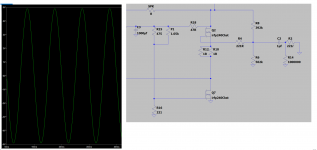
I did a little simulation of the F1 circuit configured for a single ended input in ltspice and my comment about the input capacitor (C2) on the grounded side having only DC voltage on both sides was wrong. There is AC at the junction of R6 and R8, and in the simulation this AC voltage is greatly reduced by giving it a low impedance path to ground through C2. If C2 is removed the AC voltage at this junction is much higher and the amp doesn't work. So don't remove C2.
The image F1 With C2 SE Input shows the voltage across the output with C2 in place and the negative input grounded (standard SE input configuration)
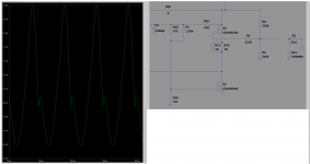
The image F1 C2 Removed shows the voltage across the output with C2 removed. Not pretty.
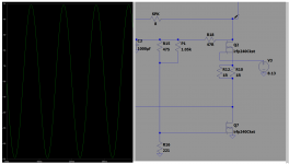
The image F1 Voltage Supply Q2 Gate replaces all of the negative side input components and the R6-R8 leg with an ideal constant voltage supply to the gate of Q2. This seems to work, although I'm not sure how much value is in the idea. Maybe it could save space, and cost if expensive input capacitors were being used.
The image F1 With C2 SE Input shows the voltage across the output with C2 in place and the negative input grounded (standard SE input configuration)
The image F1 C2 Removed shows the voltage across the output with C2 removed. Not pretty.
The image F1 Voltage Supply Q2 Gate replaces all of the negative side input components and the R6-R8 leg with an ideal constant voltage supply to the gate of Q2. This seems to work, although I'm not sure how much value is in the idea. Maybe it could save space, and cost if expensive input capacitors were being used.
Attachments
You know, there is no such thing as signal path. You hear all the parts in parallel and those going to the ground.
I agree, and after seeing that current is flowing through C2 in the simulation, I would also recommend using the same type/quality of capacitor on both the positive and negative inputs. Sorry I forgot to include this in the last post.


It is a very clean birds nest! Thanks for posting the pics, and for testing out the switching power supplies it is nice to have that option available.
A question for Nelson what is the lowest value i can use on the f1j ? as the parallel 4.3 mundorfs and the russian teflons take up too much real estate.Iwas hoping to be able to use 1uf plusa mundorf sgo 4.3 capacitor .Regards spades
You are referring to the output caps?
The only issue is that the F1J being pretty much a current source, the
output voltage before the cap will be a function of load impedance,
and low frequencies would get a pretty big boost with a small cap,
so you might find yourself clipping the amp unless you high-pass the
input as well. That value would depend on the load also, so there is
not a simple answer with the data here.
if input cap is in question, and ref. to schm in post #22 (reattached here) , Rin per phase is roughly 23K5, so for full range it calls for min. 3.3uF, taking standard value, so Mooohndorph 4.3uF as sole per phase is adequate
calc is C=1/(2*Pi*R*F)
shoot for at least octave bellow your F of interest
calc is C=1/(2*Pi*R*F)
shoot for at least octave bellow your F of interest
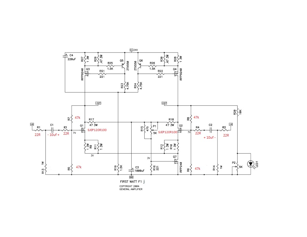
Is it important to use matched transistor pairs for the F1?
Since trim resistors can be used to achieve the desired <50mV DC offset across the speaker outputs I am wondering if matched transistor pairs for Q1-Q4 and possibly Q5 & Q6 offer improved performance or not?
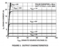
When unmatched transistors are used, and DC offset is achieved using trim resistors at R5 or R6, Q1 and Q2 will be operating at different Vgs values. Looking at the output characteristic curves for the IRFP240 the Vgs value determines which curve the mosfet is operating on. Does this difference compromise performance of the amp due Q1 and Q2 being on different operating curves? Other considerations?
Thanks for helping me learn.
Since trim resistors can be used to achieve the desired <50mV DC offset across the speaker outputs I am wondering if matched transistor pairs for Q1-Q4 and possibly Q5 & Q6 offer improved performance or not?
When unmatched transistors are used, and DC offset is achieved using trim resistors at R5 or R6, Q1 and Q2 will be operating at different Vgs values. Looking at the output characteristic curves for the IRFP240 the Vgs value determines which curve the mosfet is operating on. Does this difference compromise performance of the amp due Q1 and Q2 being on different operating curves? Other considerations?
Thanks for helping me learn.
Attachments
it is advisable to have matched Q1 and Q2, which is step in certainty of having same/similar THD spectra of both channels
though, to be absolutely certain (few more steps in direction of), matching needs to be made by xconductance, not just same Iq for Ugs
anyway, if you don't have matched SSouths, use your tricks ....... and test THD spectra after ....... if channels are not in 5% bracket, re-shuffle SSouths between channels, choose closer combination
Thanks Zen Mod🙂
I am trying to refine the F1/F1J circuit boards before placing a second order, and also pull together different pieces of information to establish a setup procedure for the amp. One of the refinements I would like to make is to add a potentiometer for adjusting the DC offset. From what I gather the following would be the preferred approach for selecting transistors and adjusting the DC offset:
- Q1 and Q2 matched for Vgs (equal Vgs creates equal Id) and transconductance (source ZM)
- Q3 and Q4 matched if you can (F1 Service Manual suggests matched)
- Q5 and Q6 matching not required
Power up amp without anything on the input or output.
Adjust P1 to achieve ~13.8 VDC at the speaker outputs
Check DC offset at speaker outputs for gross offset.
Adjust gross DC offset by adding resistance in parallel with R27/R29 or R28/R30 (adjusting here first will maintain Vgs at Q1/Q2 as close to equal as possible, also suggested in the F1 Service Manual)
Recheck VDC overall level at speaker at speaker outputs and adjust P1 for 13.8VDC.
Bring amp up to temperature and recheck DC offset. Fine tune DC offset using P3 (proposed DC offset fine tuning potentiometer that is in series with R5. (Adjustment in this location is suggested in the F1 to F1J conversion schematic from First Watt).
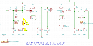
The schematic below shows where I was thinking of adding potentiometer P3, and some resistance values (for an F1 in this case) that would allow Q1 gate voltage to be higher or lower than Q2 for adjustment of DC offset in either direction.
Please let me know what you think.
Thanks again,
Chas
I am trying to refine the F1/F1J circuit boards before placing a second order, and also pull together different pieces of information to establish a setup procedure for the amp. One of the refinements I would like to make is to add a potentiometer for adjusting the DC offset. From what I gather the following would be the preferred approach for selecting transistors and adjusting the DC offset:
- Q1 and Q2 matched for Vgs (equal Vgs creates equal Id) and transconductance (source ZM)
- Q3 and Q4 matched if you can (F1 Service Manual suggests matched)
- Q5 and Q6 matching not required
Power up amp without anything on the input or output.
Adjust P1 to achieve ~13.8 VDC at the speaker outputs
Check DC offset at speaker outputs for gross offset.
Adjust gross DC offset by adding resistance in parallel with R27/R29 or R28/R30 (adjusting here first will maintain Vgs at Q1/Q2 as close to equal as possible, also suggested in the F1 Service Manual)
Recheck VDC overall level at speaker at speaker outputs and adjust P1 for 13.8VDC.
Bring amp up to temperature and recheck DC offset. Fine tune DC offset using P3 (proposed DC offset fine tuning potentiometer that is in series with R5. (Adjustment in this location is suggested in the F1 to F1J conversion schematic from First Watt).
The schematic below shows where I was thinking of adding potentiometer P3, and some resistance values (for an F1 in this case) that would allow Q1 gate voltage to be higher or lower than Q2 for adjustment of DC offset in either direction.
Please let me know what you think.
Thanks again,
Chas
Attachments
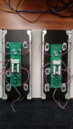
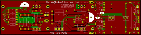
Updates to the boards for a second order are nearly complete. I have made minor tweaks based on my build and comments from adason.
Changes of note to the amp boards are:
- added a hole for wiring direct to the pads for power input and speaker output
- added P3 (a potentiometer in series with R5 to fine tuning DC offset)
- removed R105 and R106 (replaced by P3)
- added a second set of holes for using smaller resistors in parallel to create R127 and R128 for more DC offset tuning options
- decreased width of the thermal reliefs for easier soldering
- increased revision to 3.6
Changes of note to the power supply board are:
- added additional center mounting for increased support when pushing on connectors
- added a hole for wiring direct to the input/output pads
- decreased width of the thermal reliefs for easier soldering
- increased revision to 2.1
Does anyone who has a set of boards have other suggestions?
Attachments
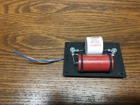
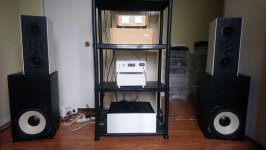
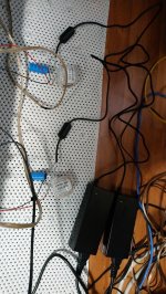
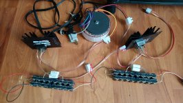
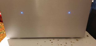
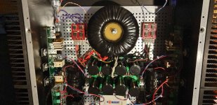
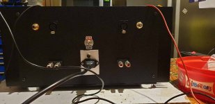
I have your previous boards they are hard to fault.Have jus finished my f1j build with these boards best sound i have ever heard from lowthers have the correction filters fitted .Here are a few pictures build not as tidy as yours and my fabrication skills are not great but the boards you supplied made the job a lot easier..So thanks a lot to you and Nelson Pass for sharing his designs .
Attachments
Last edited:
- Home
- Amplifiers
- Pass Labs
- Firstwatt F1J