Thanks! What kind of diodes, if I may ask? And, if you have anything else to contribute for the guys contemplating class-A use, please do, ...🙂
For anyone else, Please note that those are much bigger heatsinks than I have specified for class A-B (but so are the ones shown by Sergiu). A 5V drop at >1A idle current is not advisable with my $1 heatsink. For that I suggest mounting the pass transistors (at least, and perhaps the diodes also), from below w. larger heatsink, as shown in the pics above, or something similar to that shown by Salas.
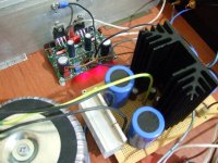
The diodes located on the back of the silver sink next to the Tx are MUR 860s. The power transistors are Toshiba 2SC5200 2SA1943 driven by BD139 BD140 in Darlington mode. The filtering is 2 stage RC (2nd order). Input & output light blue jacketed caps are F&T 10mF/63V. Trafo shown is 400VA. So you can have a scale idea for the relative sizes also.
...Class A amps won't need much Vin-Vout but will need big output capacitors, as big as the input ones. Its the high bias current that drains them fast you see, when the output current swings are mostly covered by the heavy bias and the +/- PSU voltages don't bother to sag much. Class AB needs the opposite approach.
Yes, I'm just finishing assembling the pcbs now - I didn't think about adding bigger heatsinks for the pass transistors - can stretch the legs sidewards to mount a larger 'sink on the side of the pcbs perhaps ...
Let's see - at a 4 volt drop @ 1.6A load = about 6.5W and & using a 2.5*C/W 'sink = about a 16*C temp rise above ambient - okay, at a pinch.
I have some 'sinks that are 100mm long and 55mm high so will fit along the side of the pcb but will need flying leads for the o/p wiring as terminals now blocked by heatsink - hmm.
I think if enough interest for higher power version, some pcb adjustments would be useful - we'll see just how hot this thing gets ...
Unfortunately Salas, the link on post 259 only takes me to the top of this page - could you possibly add the thread/or photo for some idea of size of the heatsink you used, please?
Go to Post 160.Yes, I'm just finishing assembling the pcbs now - I didn't think about adding bigger heatsinks for the pass transistors - can stretch the legs sidewards to mount a larger 'sink on the side of the pcbs perhaps ...
Let's see - at a 4 volt drop @ 1.6A load = about 6.5W and & using a 2.5*C/W 'sink = about a 16*C temp rise above ambient - okay, at a pinch.
I have some 'sinks that are 100mm long and 55mm high so will fit along the side of the pcb but will need flying leads for the o/p wiring as terminals now blocked by heatsink - hmm.
I think if enough interest for higher power version, some pcb adjustments would be useful - we'll see just how hot this thing gets ...
Unfortunately Salas, the link on post 259 only takes me to the top of this page - could you possibly add the thread/or photo for some idea of size of the heatsink you used, please?
edit:
The drop voltage should be higher than 50% of the expected p-p ripple voltage before the transistor. So, 4V drop would be for 8V p-p ripple, which seems unusually high for a 10 millifarad filter/reservoir cap and around 2A quiescent current plus whatever active current is added on to that. Perhaps that can be simulated, but I will check how big a load I can put on the supply. I may not get to this until Tuesday.
Moving parts around a bit is no problem.
Last edited:
Let's see - at a 4 volt drop @ 1.6A load = about 6.5W and & using a 2.5*C/W 'sink = about a 16*C temp rise above ambient - okay, at a pinch.
*Always derate published sink C/W spec by 30% due to spot heating by the semis. The spec is for even heat distribution over the entire sink's surface at optimum breathing conditions.
Unfortunately Salas, the link on post 259 only takes me to the top of this page - could you possibly add the thread/or photo for some idea of size of the heatsink you used, please?
Yes of course, here again.
Attachments
Salas, did you really need such a large voltage drop across the pass transistor, or did you just do it because you could?
I did it to be safe against low mains situations. 1.2V or more is to be covering the Darlington already anyway.
Ah, yes. So we do not need such a high voltage in our case (single mosfet, and the voltage will rise and fall naturally with high and low line with the filter characteristics intact).I did it to be safe against low mains situations. 1.2V or more is to be covering the Darlington already anyway.
...You should mind RDS times peak consumption current per rail, plus proper ripple to drop ratio at max demand.
Duncan's PSUDII free software sim will come handy to each one builder when setting for his own app I guess.
Duncan's PSUDII free software sim will come handy to each one builder when setting for his own app I guess.
Thanks guys -
I'll use some 'cut down' heavy duty sinks and add a mounting plates underneath for heatsinks support and pcb mounting - might also extend this bottom plate to include the diodes underneath for easier access to the ac input QC blades - as usual, changes before even turning it on!
I'll use some 'cut down' heavy duty sinks and add a mounting plates underneath for heatsinks support and pcb mounting - might also extend this bottom plate to include the diodes underneath for easier access to the ac input QC blades - as usual, changes before even turning it on!
If one were to use this concept for powering an 8-channel amp, 300-500 W per 4 channels, what would be the ideal setup? The amps may not all be the same draw; e.g. the tweeters will require much lower voltage than the woofers.
Almost all of a class A amp's bias current will be supplied directly through the pass transistor, not the output capacitor, so increasing its size won't help with that. On the other hand increasing the size of the input capacitor will reduce ripple, which will also reduce the required dropout voltage. Both of those effects are likely of more benefit to a class A amp than an AB one....Class A amps won't need much Vin-Vout but will need big output capacitors, as big as the input ones. Its the high bias current that drains them fast you see, when the output current swings are mostly covered by the heavy bias and the +/- PSU voltages don't bother to sag much. Class AB needs the opposite approach.
If this circuit can cope with no big capacitive aid at its output for Class A, then OK. You know its ins & outs better.
I intend to try it on a Quad 405-2 clone (ca 50 VDC in and 100 W) and some SoZ class-A compilation. We'll see how it behaves. If noone beats me which is likely cause Im slow atm
Be careful of the 50V limit. Perhaps consider a diode with higher reverse breakdown voltage than the one listed in the BOM for a margin of safety.I intend to try it on a Quad 405-2 clone (ca 50 VDC in and 100 W) and some SoZ class-A compilation. We'll see how it behaves. If noone beats me which is likely cause Im slow atm
I'll start it up easy. It worx from 42 vdc. Some smoke never hurt one that has recently given up the smokes.
I have now readed all the posts with allot of interest.. I am curious to find out (if someone could help us with a simulation) to see a comparation between this cap multiplier with the newer components (the updated version) and the one sugested by JLH hymself for his highly biased versions of class A amplifiers (from the picture from below). This would be interesting to see, because we have two circuits with potential and i think it is very importanty to see how they compare in therms of ripple, regulation, heat etc. I am really curious to see how they behave with high current eaters (like F5T, Aleph's,DoZ, JLH for Quad ESL).
Below (in the picture) are the minimum values for C1&C2 indicated by JLH for his cap multiplier.
Below (in the picture) are the minimum values for C1&C2 indicated by JLH for his cap multiplier.
Attachments

Last edited:
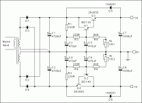
VR1 and VR2 are adjusted to give equal (but opposite) voltages on the supply rails and to give the required volt drop across the pass transistors of approximately 3V.
- Status
- Not open for further replies.
- Home
- Amplifiers
- Power Supplies
- Finished capacitance multiplier