What do you get when you measure voltage where R9 connects with P1 (ref ground)
when you adjust P1 over its entire range?
Same question for R10 and P2.
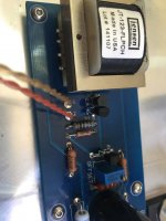
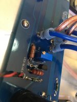
Can you post pictures of both boards?
when you adjust P1 over its entire range?
Same question for R10 and P2.
Can you post pictures of both boards?
It is Okay Zen mod.
As mentioned, the voltage at one end of R11 and R12 were far from 0 to +6V6
,tiny positive and negative.
Because I still cannot find root cause why all Mosfet dead therefore I feel be lost self-confident on what I did. It might be better to restart all with new parts.
didn't got back to your pictures , but quite possible that you have badly installed ( backwards?) LM329
anything is possible then , even dead mosfets , when you don't have proper DC voltages at gates
Voltage where R9 connects with P1 (ref ground), I can adjust from 0 to 7.15V
and R10 connects with P2 (ref ground) is from -24.8 to -17.6 V
mainly be drop in R9 and R10
and R10 connects with P2 (ref ground) is from -24.8 to -17.6 V
mainly be drop in R9 and R10
Attachments
Last edited:
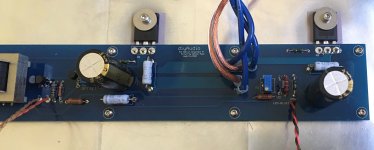
Thats parts are for snubber. More information you get on thread about Quasimodo jig.
Thanks for guidance darrr!
Thats parts are for snubber. More information you get on thread about Quasimodo jig.
As I was reading about the function of the snubber components in other threads, I found the following advice in the F5 thread:
"Build the F5 using no diode snubber...don't sweat it for now. When you have the F5 completed and your're listening to music check out the QUASIMODO THREAD."
Is this applicable for the F6 as well, can I just continue building and start listening without the snubber components and play with it afterwards?
Thanks in advance for your help!
Best Regards,
Marco Benschop
Voltage where R9 connects with P1 (ref ground), I can adjust from 0 to 7.15V
and R10 connects with P2 (ref ground) is from -24.8 to -17.6 V
mainly be drop in R9 and R10
that's good
set first one to 0V and second one to -24V8
part of your problem is that you're not realizing that exactness is important here
you've been told what to measure and how to measure , and you've done it in not exact way.......
now, when we finally got confirmation that biasing is operational, check input JFets how I described - with matching jig
As I was reading about the function of the snubber components in other threads, I found the following advice in the F5 thread:
"Build the F5 using no diode snubber...don't sweat it for now. When you have the F5 completed and your're listening to music check out the QUASIMODO THREAD."
Is this applicable for the F6 as well, can I just continue building and start listening without the snubber components and play with it afterwards?
Thanks in advance for your help!
Best Regards,
Marco Benschop
snubbers can come later
they're cherry on top
Looks like the LM329s and pots are fine.
Can't tell from the photos but can you check the clearance between PCB and
heatsink to make sure nothing might be shorting?
Can't tell from the photos but can you check the clearance between PCB and
heatsink to make sure nothing might be shorting?
snubbers can come later
they're cherry on top
Thank you Zen Mod!
Looks like the LM329s and pots are fine.
Can't tell from the photos but can you check the clearance between PCB and
heatsink to make sure nothing might be shorting?
I checked there is no shorting.
.... time to disassemble.
Thank you Dennis Hui , Zen Mod
In your post #1453 you mentioned by adjusting the pots you got about 90mV
across the gate resistors R11 and R12. You shouldn't get any real voltage
drop there. This drops corresponds to about 6.9mA, which gives you the
6.9V drop across R9/R10.
My guess is the mosfets are bad, though I have no suggestion as to why they're
all bad.
across the gate resistors R11 and R12. You shouldn't get any real voltage
drop there. This drops corresponds to about 6.9mA, which gives you the
6.9V drop across R9/R10.
My guess is the mosfets are bad, though I have no suggestion as to why they're
all bad.
In your post #1453 you mentioned by adjusting the pots you got about 90mV
across the gate resistors R11 and R12. You shouldn't get any real voltage
drop there. This drops corresponds to about 6.9mA, which gives you the
6.9V drop across R9/R10.
My guess is the mosfets are bad, though I have no suggestion as to why they're
all bad.
Thank you Dennis Hui,
I got experience ....should also check all active parts before assemble.
Hello All,
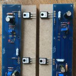
I have a question about the IRFP240’s for Q1 and Q2.
Should I solder the matched pairs to 1 channel, or should I solder the matched pairs to the same location on each channel (for example one matched pair to both Q1’s and one matched pair to both Q2’s)?
Please see the photo attached for reference.
Thank you!
Attachments
Hello All,
I have a question about the IRFP240’s for Q1 and Q2.
Should I solder the matched pairs to 1 channel, or should I solder the matched pairs to the same location on each channel (for example one matched pair to both Q1’s and one matched pair to both Q2’s)?
Please see the photo attached for reference.
Thank you!
Kind of depends how different the matched pairs are to each other, and what you want to achieve.
When I say matched I am not referring to Vgs values at the required bias point but how matched are the curves of Id vs Vgs (ie transconductance values)
Last edited:
^ This is an interesting question. I might suggest that the matched pairs be used in the same location in each channel. This could improve the matching of performance between the two channels, and therefore imaging.
One matched pair for Q1 and Q2 per channel.
Thank you for your reply.
Is there any reason why?
^ This is an interesting question. I might suggest that the matched pairs be used in the same location in each channel. This could improve the matching of performance between the two channels, and therefore imaging.
That’s the feeling I have too, the channels become more identical when using the matched ones in the same location at each channel, thus better stereo.
Acoustic emotion - for all practical purposes, that is a matched quad of Mosfets. Use wherever you like. 🙂
Also, F6 does not require tight matching in Mosfets.
Also, F6 does not require tight matching in Mosfets.
Acoustic emotion - for all practical purposes, that is a matched quad of Mosfets. Use wherever you like. 🙂
Also, F6 does not require tight matching in Mosfets.
Thanks, all clear now 🙂
- Home
- Amplifiers
- Pass Labs
- F6 Illustrated Build Guide