I'm using LM329 voltage references in my F6. They work quite well. My power rails are +/– 26.4V, R7 and R8 are 3.9k Ohms, to make sure there is plenty of current feed the 5k trimmer resistors and the LM329s.
It might be good to make sure that the 329s have been connected with the correct pins and polarity.
It might be good to make sure that the 329s have been connected with the correct pins and polarity.
Last edited:
Dunnno ..attempting to 'improve' the Pass design does open up serious
bungle opportunities.
If these improvements were.. genuinely worthwhile... wouldn't they be in the original design ??
bungle opportunities.
If these improvements were.. genuinely worthwhile... wouldn't they be in the original design ??
Dunnno ..attempting to 'improve' the Pass design does open up serious
bungle opportunities.
If these improvements were.. genuinely worthwhile... wouldn't they be in the original design ??
Well , everything is upgradable by nature , fact is that the LM329 works at TungstenAudio , and that's what I like to know 😉
.
Dunnno ..attempting to 'improve' the Pass design does open up serious
bungle opportunities.
If these improvements were.. genuinely worthwhile... wouldn't they be in the original design ??
The "modification" to the bias (LM329 and 3k3 resistor
are suggested and explained early on the F6 build thread.
This works very well in my F6.
The "modification" to the bias (LM329 and 3k3 resistor
are suggested and explained early on the F6 build thread.
This works very well in my F6.
Mine also.
The purpose here is to establish a low noise voltage reference of which the lm329 is certainly up to the task.
What ever part is chosen in this location, making sure the voltage reference is fed adequate current, should be the primary concern.
What ever part is chosen in this location, making sure the voltage reference is fed adequate current, should be the primary concern.
Hi I checked on other channel. It has exactly the same issue.
Please advise me ,what I should check or take measure before dismantle all four mosfet ?
thank you
Please advise me ,what I should check or take measure before dismantle all four mosfet ?
thank you
remove mosfets , power it up , confirm all voltages
then put new mosfets , taking care of everything already said
be sure that trimpots are in al the way down position , sending 0V to mosfet gates , ref. to adjacent source
if needed , ask for more clarification
then put new mosfets , taking care of everything already said
be sure that trimpots are in al the way down position , sending 0V to mosfet gates , ref. to adjacent source
if needed , ask for more clarification
remove mosfets , power it up , confirm all voltages
then put new mosfets , taking care of everything already said
be sure that trimpots are in al the way down position , sending 0V to mosfet gates , ref. to adjacent source
if needed , ask for more clarification
Thank, Zen mod. I will when new set arrived.
I measured voltage S-D at K170 and J74 ,they are same as source power supply 25 V and there is no voltage on 1-3 ,2-4 at xformer.
K170 and J74 are still okay, aren't they?
Thank, Zen mod. I will when new set arrived.
I measured voltage S-D at K170 and J74 ,they are same as source power supply 25 V and there is no voltage on 1-3 ,2-4 at xformer.
K170 and J74 are still okay, aren't they?
measure voltage across R18
then , ref. to GND , measure voltage at any end of R11 , and confirm max and min voltage at R11 which you can set with P1
same logic , ref. to negative rail , measure voltage at any end of R12 , and confirm max and min voltage at R12 which you can set with P2
ref. means - black probe goes there
You said to measure voltage across R18. I believe you mean R4 18 ohm (I used 20 ohms in my F6.)
I measured voltage at the end to mosfet gate for R11 and R12 , when measured I would try to set other POT in middle span.
Right Channel
R11 ref. to GND
Min 6.6 mV (voltage across R11 near zero) and voltage across R4 = -7.0mV
Max 126 mV (voltage across R11 = 92mV) and voltage across R4 = 1.2 mV
R12 ref. to negative rail
Min 66.5 mV (voltage across R12 near zero) and voltage across R4 = -1.9mV
Max 133 mV (voltage across R12=93mV) and voltage across R4 = -3.0mV
Left Channel
R11 ref. to GND
Min -166 mV (across R11 near zero) and voltage across R4 = -21.0mV
Max -40 mV (across R11 = 93.8mV) and voltage across R4 = -11.5 mV
R12 ref. to negative rail
Min 59.6 mV (cross R12 near zero) and voltage across R4 = -16.7mV
Max 98 mV (voltage across R12=89 mV) and voltage across R4 = -18.5.0mV
Thank you
Last edited:
You said to measure voltage across R18. I believe you mean R4 18 ohm (I used 20 ohms in my F6.)
I measured voltage at the end to mosfet gate for R11 and R12 , when measured I would try to set other POT in middle span.
Right Channel
R11 ref. to GND
Min 6.6 mV (voltage across R11 near zero) and voltage across R4 = -7.0mV
Max 126 mV (voltage across R11 = 92mV) and voltage across R4 = 1.2 mV
R12 ref. to negative rail
Min 66.5 mV (voltage across R12 near zero) and voltage across R4 = -1.9mV
Max 133 mV (voltage across R12=93mV) and voltage across R4 = -3.0mV
Left Channel
R11 ref. to GND
Min -166 mV (across R11 near zero) and voltage across R4 = -21.0mV
Max -40 mV (across R11 = 93.8mV) and voltage across R4 = -11.5 mV
R12 ref. to negative rail
Min 59.6 mV (cross R12 near zero) and voltage across R4 = -16.7mV
Max 98 mV (voltage across R12=89 mV) and voltage across R4 = -18.5.0mV
Thank you
yes, measure across R4 (R18 was a typo)
you need to see action , from 0V to what is LM329 giving max (6V6 to 7V2)
Last edited:
Hello Guys,
Quick question about the PSU for an F6, because I got stuck.
I am a bit confused about the values for the following parts, and if they are needed at all to use (because the BOM of the PSU says it is different per application and since I am new to electronics I am not sure what to do).
- RS1 + 2
- CX1 + 2
- CS1 + 2
Please see the photo attached.
Which values should I use for these components, or should I not use them at all?
I am going to use a 500va (18v + 18v) transformer.
Any help is much appreciated!
Best Regards
Happy New Year everyone...
I have an unusual observation which I wanted to share & understand, but unfortunately I don't have temperature readings to share for now...When I run F6 with 8 ohm speakers, the amp runs a bit warm (I am using the Deluxe 5U Alu chassis), but when I plug in 4 ohm speakers, the amp run way cooler, the heatsink can be barely termed as warm or probably room temperature...I was to believe it should have been the other way around. The room temperature is around 21C. I will try get a thermometer to share temp. details soon...Any guesses why?
I have an unusual observation which I wanted to share & understand, but unfortunately I don't have temperature readings to share for now...When I run F6 with 8 ohm speakers, the amp runs a bit warm (I am using the Deluxe 5U Alu chassis), but when I plug in 4 ohm speakers, the amp run way cooler, the heatsink can be barely termed as warm or probably room temperature...I was to believe it should have been the other way around. The room temperature is around 21C. I will try get a thermometer to share temp. details soon...Any guesses why?
Thats parts are for snubber. More information you get on thread about Quasimodo jig.Hello Guys,
Quick question about the PSU for an F6, because I got stuck.
I am a bit confused about the values for the following parts, and if they are needed at all to use (because the BOM of the PSU says it is different per application and since I am new to electronics I am not sure what to do).
- RS1 + 2
- CX1 + 2
- CS1 + 2
Please see the photo attached.
Which values should I use for these components, or should I not use them at all?
I am going to use a 500va (18v + 18v) transformer.
Any help is much appreciated!
Best Regards
Happy New Year everyone...
I have an unusual observation which I wanted to share & understand, but unfortunately I don't have temperature readings to share for now...When I run F6 with 8 ohm speakers, the amp runs a bit warm (I am using the Deluxe 5U Alu chassis), but when I plug in 4 ohm speakers, the amp run way cooler, the heatsink can be barely termed as warm or probably room temperature...I was to believe it should have been the other way around. The room temperature is around 21C. I will try get a thermometer to share temp. details soon...Any guesses why?
A Class amp is running full throttle ( regarding current, thus dissipation) all the time , transferring all the heat in heatsinks without signal
when you are actually putting some signal in , and amp is doing its job with speakers , energy is practically taken away from output transistors (heat in idle) and transferred to speakers
generally 4R load is needing more current that is the case with 8R
so that's it
yes, measure across R4 (R18 was a typo)
you need to see action , from 0V to what is LM329 giving max (6V6 to 7V2)
Yes, I can see their action as last measurement.
Right Channel
when measured R11 ref. to GND then turn P1
Voltage across R4 is move from -7.0mV to 1.2 mV
when measured ref. to negative rail then turn P2
Voltage across R4 is move from -1.9mV to -3.0 mV
Left Channel
when measured R11 ref. to GND then turn P1
Voltage across R4 is move from -21.0 mV to -11.5 mV
when measured R12 ref. to negative rail then turn P2
Voltage across R4 is move from -16.7 mV to -18.5 mV
about above resulted tell something?
sorry , I made a mistake ( more than once) , thinking all the time about checking JFet current at R4 ...... R4 practically showing just difference between JFets if they're not perfectly matched
must be not enough coffee these days
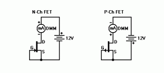
you need to check input JFets with simple matching jig , so - yes - desoldering them from circuit
on the other hand , what I wrote about P1 and P2 and associated tests - that's having nothing with R4
measure voltage between R11 and GND , while moving P1 from end to end , and write what you have ; for proper operation of biasing circuit associated with upper mosfet , you need to see voltage span from 0V to +6V6
measure voltage between R12 and negative rail , while moving P2 from end to end , and write what you have ; for proper operation of biasing circuit associated with lower mosfet , you need to see voltage span from 0V to +6V6
must be not enough coffee these days
you need to check input JFets with simple matching jig , so - yes - desoldering them from circuit
on the other hand , what I wrote about P1 and P2 and associated tests - that's having nothing with R4
measure voltage between R11 and GND , while moving P1 from end to end , and write what you have ; for proper operation of biasing circuit associated with upper mosfet , you need to see voltage span from 0V to +6V6
measure voltage between R12 and negative rail , while moving P2 from end to end , and write what you have ; for proper operation of biasing circuit associated with lower mosfet , you need to see voltage span from 0V to +6V6
Attachments
Last edited:
It is Okay Zen mod.
As mentioned, the voltage at one end of R11 and R12 were far from 0 to +6V6
,tiny positive and negative.
Because I still cannot find root cause why all Mosfet dead therefore I feel be lost self-confident on what I did. It might be better to restart all with new parts.
As mentioned, the voltage at one end of R11 and R12 were far from 0 to +6V6
,tiny positive and negative.
Because I still cannot find root cause why all Mosfet dead therefore I feel be lost self-confident on what I did. It might be better to restart all with new parts.
- Home
- Amplifiers
- Pass Labs
- F6 Illustrated Build Guide