I'm still wondering about driving the input JFETs with +-30V rails.
You'll kill the JFets. Been there done that. I'm currently running the Cree SiC outputs in my F6 version on 35V rails and use super regulators on the input buffer to get the voltage down to 20V.
You'll kill the JFets. Been there done that. I'm currently running the Cree SiC outputs in my F6 version on 35V rails and use super regulators on the input buffer to get the voltage down to 20V.
ok!! Thank you for saving me from an expensive experiment 🙂
Researching super regulators right now.
BTW, why did you go for the Cree SiCs? Would you have a pointer to some discussion etc?
Thanks so much -- LATB
I used them because I had them and they seemed to make sense for that build. As built I didn't like my F6 much. Some modifications helped. Maybe it would have been easier with the originally speced parts but I doubt it.
You don't need to use Jung/Didden Superregs, any regulators or resistive voltage dividers will do as a start.
You don't need to use Jung/Didden Superregs, any regulators or resistive voltage dividers will do as a start.
My F6 power rails were +/– 26V, but the standard F6 input stage doesn't have any source degeneration on the JFets. I used a variation of the Austin input stage that is included with the M2x. The Austin IPS is a version of what is commonly known as a diamond buffer. It can be readily adapted to drive the F6 in place of those two lonely JFets. I built it on a veroboard like so:
Attachments
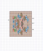
My F6 power rails were +/– 26V, but the standard F6 input stage doesn't have any source degeneration on the JFets. I used a variation of the Austin input stage that is included with the M2x. The Austin IPS is a version of what is commonly known as a diamond buffer. It can be readily adapted to drive the F6 in place of those two lonely JFets. I built it on a veroboard like so:
This is great! Out of curiosity, is that veroboard illustration a rendering option in Kicad, eagle, etc, or something you created one-off? I’ve just started dabbling in Kicad and don’t know much about anything yet 😀
That veroboard drawing was done in an iPad app called StripboardCAD. It follows the same conventions used on the Guitar FX Layouts website. It's also possible, though somewhat tedious, to do a strip board layout using graph paper and colored pencils. That's how I did many of my first custom bass guitar pedals.
These days I can read a layout the same as one would read the code of the Matrix 😉
These days I can read a layout the same as one would read the code of the Matrix 😉
TungstenAudio, what is the advantage of using the diamond buffer in place of those two jfets?
The way this version of the diamond buffer is constructed allows it to operate at higher rail voltages without stressing the components. The input transistors are fed from CCS which use 10V references. This keeps the bipolar transistors running in a safe region for voltage and current. If I understand correctly, this was Mark Johnson's contribution for the 'Austin' input stage. I kept this the same, and tweaked the output stage to use more robust Toshiba bipolar output transistors. These are the TTC004B and TTA004B, which use the TO-126 package. I also added 10 Ohm Base stoppers and reduced the Emitter degeneration to 10 Ohms for those output transistors.
During initial evaluations of my M2x with different input buffers, the Austin emerged as my overall favorite after trying several other types, including the Ishikawa which is essentially the same as the input buffer of the standard F6 (and M2). I noticed a similar sonic signature to my F6 as I was making adjustments to its bias settings, and have been very pleased with the way it sounds.
The attached schematic shows the Austin IPS as it is implemented for the M2x. This should give a good idea of how the circuit works.
Attachments
My F6 power rails were +/– 26V, but the standard F6 input stage doesn't have any source degeneration on the JFets. I used a variation of the Austin input stage that is included with the M2x. The Austin IPS is a version of what is commonly known as a diamond buffer. It can be readily adapted to drive the F6 in place of those two lonely JFets. I built it on a veroboard like so:
that's a great idea -- I actually bought the M2X boards, and will experiment a bit.
Random observation: not a good idea to just leave out the JFETs while doing the Bias adjustments: R3 suddenly started to get very hot, which really confused me because the voltage across it never got above a few 10s of mVDC.
Thinking about it a bit, with the Tx primary open, I suppose there was a high frequency feedback pumping a few watts into poor R3...
I put a bridge across gate and source of Q3 -- that fixed it.
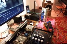
Next: connect in and output and listen to some music (mono only, for the moment...).
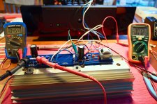
BTW: turns out my rails are at ~26V, so I'll probably going to be fine with the JFETs after all. At a bias of ~1A the heatsink stays at a toasty 50C.
I noticed that bias and offsets are wandering around quite a bit when everything warms up. More disconcertingly, when I switch on the output shows voltage swings around up to a couple of Volts. Hope my speakers don't choke on that when I connect them...
Thanks for all the input so far! LatB
Attachments
 btw cute psu transformers.
Always fun to hear music playing from one's own creation. 🙂
You mentioned that you have been seeing fluctuations in your offset voltages, and that the heatsinks are a somewhat toasty 50 °C. These things are related to each other. The biasing scheme of the F6 is susceptible to the temperature coefficients of its output devices and voltage references. Since your heatsinks are a little on the small side, and are out in the open, instead of attached to the side of your chassis, they create convection currents in the air around them. This leads to small changes in the bias voltage, which in turn cause temperature fluctuations in the output Mosfets, which create more convection, etc.
Your F6 would benefit from larger heatsinks, which are the most frequent recommendation from many DIY enthusiasts. Enclosing the interior side of your heatsinks with your chassis would help stabilize the air temperature around the biasing networks. You may also want to look at different options for the devices you are using for the voltage references. Zener diodes above 5.1V have a positive tempco, the same as the big Mosfets. The LM329 buried zener references have a near-zero tempco, and little green LEDs have a negative tempco.
My F6 uses a conventional aluminum chassis which I reinforced to handle more power dissipation. The heatsinks I used are 140mm high, 400mm long and 45mm wide. They are in good thermal contact with the heavy front plate and also the base plate, due to the added reinforcement. This configuration lets me run a bias current of 1.85 Amps while the heatsinks are nice and warm, but safe to touch. The amp does take over an hour to reach thermal equilibrium, after which the voltages and currents remain stable.
This build still has the LM329 voltage references, but I have sets of green LEDs and E-562 current reference diodes on hand to switch to a negative tempco scheme for the bias networks. The idea is to be able to start with a bias current that is closer to the final value under thermal equilibrium. I'd like to have the amp ready to play in 20 minutes, instead of an hour plus.
Last edited:
yup, you’re right I need more and better cooling. With this sink I can’t sustain more than ~0.85A. I’m looking for something better.
Thanks also for the ideas for bias thermal compensation, I’ll look into that, too.
Thanks also for the ideas for bias thermal compensation, I’ll look into that, too.
Power supply in and running. Used an Antek 4220 which gives me about 27.5 volts on both sides. Shut power down to watch green LEDs go dark. Oppps there still lit, further observation I used 22k as bleeder resistors not 2.2k Oppps. Will get them changed out and move on. I'm assuming 27.5 volts is ok to run at. All caps are 35 volts or higher.
And, the diyaudiostore PSv1.3 BOM shows 4.7k to 22k which is why mine does the same thing.🙂
I guess I will leave it 22k. I had a hand written list, one showing 22k and another showing 2.2k. I think the other list was for an older power supply board that I used in my F5. Maybe I should follow the old woodworking saying , measure twice and cut once, or check BOM twice and order once.
- Home
- Amplifiers
- Pass Labs
- F6 Illustrated Build Guide