I just purchased some (50) 2sk170GR from zhoufang off ebay he a member here. They fell in half in the 6 to 7 range and rest in 7 to 10ma range. Hope this will help you.Hi,
i have some parts for the f5x at home and want do build one. I have a few 2sj74 with Idss between 5.4 and 6.4 mA und a few 2sk170 with Idss between 7 and 11 mA. Can i degenerate the 2sk170 instead of the 2sj74? Is it a good option?
Many thanks for your help!
Daniel
GR grade shouldn't be that high of the idss ..... The readings are more like BL.I just purchased some (50) 2sk170GR from zhoufang off ebay he a member here. They fell in half in the 6 to 7 range and rest in 7 to 10ma range. Hope this will help you.
There are capacitors on board, and they will have a surge current at start up.
I have no good idea how you can test circuits without a lab supply with current limit.
But the guy who designed and tested the board is near you, so why don't you get in touch ?
But you should really post your build questions in the build thread.
These are all not design related issues.
Patrick
I have no good idea how you can test circuits without a lab supply with current limit.
But the guy who designed and tested the board is near you, so why don't you get in touch ?
But you should really post your build questions in the build thread.
These are all not design related issues.
Patrick
Patrick this is the build thread.
You initially had an idea of using fuses over the secondaries, that is at least some idea.
The circuit is Xens responsibility, I'm personally fed up with the double handling of this botched process between Alexis, Xen and yourself.
No I do not want to contact Alexis, I'd rather have it here in the build thread for all to see and benifit from, that's the whole point, to share, benifit as a community.
Ask away here then. Please also give a high resolution photograph of both sides of the board so that each IC is clearly visible.
Please also check if there is a short on either the +5V to gnd, +12V to gnd and +24V to +12V
Please also check if there is a short on either the +5V to gnd, +12V to gnd and +24V to +12V
John,
There is no need to air your frustration on me.
> The circuit is Xen's responsibility,
Yes, it is, and it is proven to work as intended. See Greg's example.
But I do not think it is my responsibility to nurse every builder's project through, if they do not have the necessary equipment & the know how to test.
The circuit is fully documented, as is the description and test procedure.
If you take time and effort to understand how it works, there is no reason why you cannot trace any building (as opposed to design) bugs.
On top of that, there is no way anyone can do remote debugging for you.
I have made a practical proposal to you to solve your problem, if there is one in the first place.
If you had a lab supply with current limit, you would have been able to charge the capacitors under a controlled manner.
Any soldering fault will appear as a short circuit, and the voltage cannot build up.
Without a lab supply, and a digital multimeter, and an oscilloscope, how would you be able to build the amplifier itself ?
Patrick
Last edited:
I just chatted to Alexis.
He called you, but you did not answer.
He lives close enough to you and is willing to help you through the test.
Why not trust his generosity once ?
Patrick
He called you, but you did not answer.
He lives close enough to you and is willing to help you through the test.
Why not trust his generosity once ?
Patrick
Thanks Patrick, I have contacted Alexis.
I have clearly been out of line, for that I apologise. I’ve taken my frustrations out on the people who have put in the most effort.
JBdV yes slow blow.
I have clearly been out of line, for that I apologise. I’ve taken my frustrations out on the people who have put in the most effort.
JBdV yes slow blow.
You are correct sorry for the error they where bl . However they are as stated in the range he was looking for thanks for the correction.GR grade shouldn't be that high of the idss ..... The readings are more like BL.
I've finished testing my (R4) protection board.
It operates perfectly under test as described in the PDF document.
Thanks Alexis and Patrick!
It operates perfectly under test as described in the PDF document.
Thanks Alexis and Patrick!
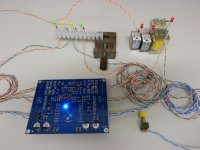
Protection Board Alive
Today our first protection board became alive.
Fixing the startup sequence with the wire bridge was a bit tricky,
but with some patience (and a magnification lens) no problem.
First time right, everything works as expected:
Start up sequence: checked
Speaker protection trip: checked
I guess that´s not too bad, all three of us made their first SMD soldering experiences with this board. Lucky beginners or naturals 🙂
But more important at this point, congrats to the designers.
Markus
Attachments


Very well done Markus!
I now have both amp channels up and running with floating X connections, I’m getting fairly close.
Recently I’ve been working on final wiring, I drew up a diagram to visualise physically, before I start. I have a couple of queries if I may.
1) The regular pcb and schematic have 3 connections for J2 when only 2 are needed (+ and -), what is the middle floating connection intended for?
2) The wire run needed to make a series connection in my diagram for the daughter board relays will run around the amp. Is there a better way of implementing this?
See diagram link below.
https://drive.google.com/file/d/0B5kI-G-h_GXkdUxmQVlheXp6VGs/edit?usp=sharing
Many thanks for a very enjoyable project.
Congratulations to Markus & gang. 🙂
As to John's questions :
1) If you refer to the relay pins at the regulator, then the middle has no connection. I like using 3 pins to give it a bit more separation. No other reasons.
2) If you wish to use 12V relays and wire them in series, you should only use ONE of the two relay outputs to drive them (either left channel or right channel, but not both). For the input shunt relays, you just run two wires per relay to the front panel. Then the negative of Relay 1 goes to the protection board relay -ve (e.g. ISR1B), the positive is connected to negative of relay 2, and the positive of relay two to the positive of the protection board (same) relay +ve (ISR1A). The amount of wire is almost the same as using 24V relays.
Of course you now need to supply twice the current from the same relay driver (which is not a problem). And the wiring is a touch messy. But no reason it should not work.
The relay driving MOSFETs are not matched, so DO NOT parallel two relay outputs together. Even worse is as you have drawn, where you essentially short circuited them. Please check through the schematics of Alexis and try to understand for yourself.
Of course no such issues if you use 24V relays instead.
Patrick
Patrick, I understand my mistake and source of initial confusion. I will refer back schematics for solid understanding.
The diagram has been revised accordingly.
You’ve saved my bacon answering this. Thank you so much for your time I really appreciate you and the Xen teams hard work.
Cheers
John
The diagram has been revised accordingly.
You’ve saved my bacon answering this. Thank you so much for your time I really appreciate you and the Xen teams hard work.
Cheers
John
Now it should be OK. 🙂
You may also use LSP2+ instead of LSP1+ (only + as they are all common) if it makes life easier.
Refer back to the schematics of Alexis.
Patrick
You may also use LSP2+ instead of LSP1+ (only + as they are all common) if it makes life easier.
Refer back to the schematics of Alexis.
Patrick
- Home
- Amplifiers
- Pass Labs
- F5X -- the EUVL Approach - The Build Thread