Just joking......🙂
These are fakes that I picked up on the way🙁
Perfect for practicing😉
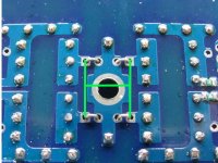
Back to business: from what I can see/measure the inner set of holes on the PCB will make the best fit (or bending will have to exceed 90˚)
Cheers,
Nic
That gave me the best laugh of the day - thanks Nic! I particularly like the one on the right with the legs bent in different directions...
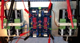
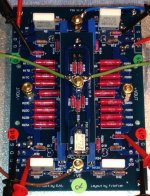
Front-end biasing
Ok - I'm ready to plug in mosfets🙂
Of (possibly) useful note I found that:
1) It is highly recommended to dial in the Vgs voltage before soldering in the MOSFETs. With the factory "settings" of the trim-pots I would have had 2.8V Vgs on my MOSFETs which would have caused a current draw way exceeding several ratings of this amp (possibly frying the MOSFETs to start with). I dialed the Vgs down to 2.15V (0.15V below the measured Vgs@2A for my FETs) thinking that this will yield about 1.5A bias current.........
2) There are two rows of holes for the MOSFETs. I soldered in a small solder tag in the free source hole as this is very practical for clipping on a voltmeter probe when biasing.
In the photos please ignore:
Cap orientation in the CAP banks - it is wrong🙁
Wire colors🙁
Sorry about the photo quality. I'm still hoping Patrick can help me getting my hands on a Leica for a fair price🙂
Cheers,
Nic
Attachments
re the 0.1uF capacitors. I am certain that I shipped you 1uF caps. if I did ship you 0.1uF caps though it would not be a problem to use them in place anyway.
re post #229: the mute boards use a NO relay and as such they should be open without the relay. the HJ4002 are in fact the markings on the 74HC4002, as far as my knowledge, they are the part on my prototype and work well.
Re post #304: I will post a more in depth explanation once I have finished an EE assessment I have due monday.
error in amp BOM
In the amp BOM the two P MOSFETs are designated Q1 and Q8. I think this should be Q1 and Q6. Q8 is a JFET and the PCB is correctly labeled.
I may have an old BOM and I did not check the schematics.
Q: In amplifier/circuit jargon what does "top" and "bottom" refer to?
Are "opposite corners" referring to top-left versus bottom-right?
I'm just trying to understand the terminology of the excellent bias description by Dave.
magic moment...Nic no ? ufff !!! hehehe.
Let us know how it sounds later on.😀
After about 1 hour of warming up and without adjusting anything I get:
378, 378, 379 and 379 mV drop over 0.22R (= 1.72A bias)
3.5 and 0.6 mV offset on the outputs.
Heatsink: 53˚C
I guess I can be happy with this even if I had been calculating to hit 1.5A (and not 1.7A).
I guess having MOSFETs measured at operating temperature also has some practical advantages😎
I will later dial it up to 2A and then maybe learn to use my PicoScope to find out if this is indeed an amplifier and not just an expensive heating block🙄
One question: if the current is essentially equal for all 4 quadrants, how will I come about adjusting down offset on the outputs😕
I'll have to let Dave answer those questions as it is his documentation and numbering system ....
Sorry,
Patrick
Sorry,
Patrick
How equal are your currents, to mA ? Even 1mA x 8R load is 8mV.
If you have no load, any imbalance in current even in mA has no where to go other than the feedback network.
So you still need to adjust for zero voltage offset.
That is why the trimmers are there.
You can pick any one you want, as long as in the end the offsets are zero.
Otherwise good progress.
Patrick
>How equal are your currents, to mA ? Even 1mA x 8R load is 8mV.
On the outputs? The outputs are loaded with 4.7R dummy resistors. I have 3.5 mV and 0.6 mV offset so that would be 0.74mA and 0.13mA flowing here.
So the goal is to achieve zero output offset even if this results in slightly different bias currents?
On the outputs? The outputs are loaded with 4.7R dummy resistors. I have 3.5 mV and 0.6 mV offset so that would be 0.74mA and 0.13mA flowing here.
So the goal is to achieve zero output offset even if this results in slightly different bias currents?
> Let us know how it sounds later on.😀
Is that important😀
Looooooong way to go. The F5X has a component density comparable to an iPhone and I still have to find out how to squeeze it all in there.
Is that important😀
Looooooong way to go. The F5X has a component density comparable to an iPhone and I still have to find out how to squeeze it all in there.
Yes.
I assume you have grounded X.
After you float the X (or perhaps even you might use the H as published by NP in F5T and also discussed in F5XP article), you will need to readjust anyhow.
But the aim is indeed zero voltage offset at bias and temperature on both outputs relative to Gnd.
Patrick
I assume you have grounded X.
After you float the X (or perhaps even you might use the H as published by NP in F5T and also discussed in F5XP article), you will need to readjust anyhow.
But the aim is indeed zero voltage offset at bias and temperature on both outputs relative to Gnd.
Patrick
> The F5X has a component density comparable to an iPhone and I still have to find out how to squeeze it all in there.
Compared to the iphone ?
Tones of space.
🙂
Patrick
Compared to the iphone ?
Tones of space.
🙂
Patrick
BTW I suggest you use min. 1.5mm2 silicone flexible test leads for your power wiring.
Preferably 2.5mm2.
You pass constantly 4A through them after all.
Patrick
Preferably 2.5mm2.
You pass constantly 4A through them after all.
Patrick
> After you float the X (or perhaps even you might use the H as published by NP in F5T and also discussed in F5XP article), you will need to readjust anyhow.
I have read NPs F5T and your F5XP articles, but it is not clear to me how the H configuration would be implemented on the F5X amp boards. Can this simply be done using jumpers?
I now have the amp (in grounded X configuration) dialed in to 2A bias with <1 mV dc offset on the outputs. The sink is 60˚C and I am considering to bias a bit lower (1.8A?) as live a place where 28˚C is a normal room temperature good part of the year.
I will float the amp later when the supplies and the rest is ready.
Nic
In the amp BOM the two P MOSFETs are designated Q1 and Q8. I think this should be Q1 and Q6. Q8 is a JFET and the PCB is correctly labeled.
I may have an old BOM and I did not check the schematics.
...
That should be already known to Dave.
http://www.diyaudio.com/forums/pass-labs/208880-f5x-euvl-approach-build-thread-17.html#post3243644
For this reason, I wrote "Q6(Q8)" in the spreadsheets accompanying the MOSFETs in the GB.
- Home
- Amplifiers
- Pass Labs
- F5X -- the EUVL Approach - The Build Thread