Glad it's an easy fix and no loss to sound quality. Thanks for the quick reply. I'm ready to get this amp running at 100%.
Hello,
Can someone please confirm this..
1) The F5t v3 store-bom says "per channel", to me that means order double to get 2 monoblocks, right?
2) Resistors R31-R42 is for a 3rd set of output boards, same for the Mur3020s D5-D8 right?
Thank`s
Can someone please confirm this..
1) The F5t v3 store-bom says "per channel", to me that means order double to get 2 monoblocks, right?
2) Resistors R31-R42 is for a 3rd set of output boards, same for the Mur3020s D5-D8 right?
Thank`s
Finally,
F5 Turbo V2 is cooking!
For now Bias is set to .31 V and offset is fluctuating between -2 an +2 mV
the Right channel voltage difference over the Source resistor is .001 V however the Left Channel is .005 V difference. No Worries I think.
it's still possible to hold my hand on the heatsink without the urge to remove is after a minute or so, nice and cosy.
Amp is build in a 5U Deluxe using a 800VA transformer.
Attachments
Finally,
F5 Turbo V2 is cooking!
For now Bias is set to .31 V and offset is fluctuating between -2 an +2 mV
the Right channel voltage difference over the Source resistor is .001 V however the Left Channel is .005 V difference. No Worries I think.
it's still possible to hold my hand on the heatsink without the urge to remove is after a minute or so, nice and cosy.
Amp is build in a 5U Deluxe using a 800VA transformer.
Nice build!
What is your transformer voltage.
It was difficult to start up or set up the amp?
Thank you
Nice build!
What is your transformer voltage.
It was difficult to start up or set up the amp?
Thank you
Transformer is an Amplimo 2x 25V secondary 800 VA giving a 34V rails.
If you take care and turn the P1 & P2 with ease it is not hard to set-up.
Use the F5Turbo Illustrated guide and it will probably go ok!
Nils
Folks:
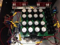
As much as I have enjoyed my F5T V3 monoblocks over the past 15 months or so, I was a little disappointed that they lacked some of the authority and weight that the Aleph 1.2 monoblocks they replaced had in spades. I had hoped that fiddling with P3 would work, but that effort proved ill-fated (see http://www.diyaudio.com/forums/pass-labs/267431-f5-turbo-3-failure.html). Instead of gambling against the odds a second time, I spent part of this past weekend adding another 90,000 uF (and a 0.5R / 50 watt resistor) to the stock-sized power supply in each amp, bringing the total to 250,000 uF per monoblock. The power supply capacitors (twenty-two per amp) are all Nichicon KG. This won't come as a surprise to most of you, but the results are terrific -- there is no bloat, the amps still sound neutral, fast and dynamic and my V3s are more commanding and engaging than before. Highly recommended!
Peace and love, peace and love.
Regards,
Scott
Glad to hear that you got it sorted to your satisfaction.
Could you provide a bit of detail? How did you add to the original CRC config? More caps and a .5R resistor where?
Thanks. Nash
The bias voltage is the Vgs of the output mosFET plus the V of the source resistor......................
the Right channel voltage difference over the Source resistor is .001 V however the Left Channel is .005 V difference. No Worries I think. ................
The Source resistor voltage, Vse, sets the output bias current.
The Vgs is set by the make up of the transistor. You have no control over that. It is what is comes as.
Difference between P & N Vgs is of no concern.
When you measure a small difference of Vse (after setting offset to zero), you are actually measuring a small difference in resistor value.
These resistors should be matched before assembly. I aim for <<1% error and preferably around 0.1% tolerance, so that measurements later have no doubt about what they mean.
Glad to hear that you got it sorted to your satisfaction.
Could you provide a bit of detail? How did you add to the original CRC config? More caps and a .5R resistor where?
Thanks. Nash
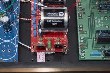
Nash:
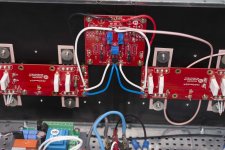
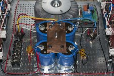
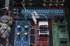
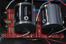
I added a third stage to the power supply in each monoblock; see the first photo. The third stage consists of six 15,000 uF capacitors and a pair of 0.5R/50W resistors (which arguably weren't necessary). A six position terminal block was used to organize the connections going to the new third stage (from the existing power supply board) and to the F5T pcbs (from the third stage). I redirected the "output" from the existing power supply pcb (see the second photo) that had previously gone to the F5T pcbs to the first, third and fifth positions on the terminal block (the first position is at the top), which then fed the three capacitors on each rail of the third stage. The output from the final capacitors on each rail in the third stage go to the second, fourth and sixth positions on the terminal strip, and then on to the F5T pcbs.
I hope that makes sense. If not, I'd be happy to try it again.
Regards,
Scott
Attachments
Nash:
I added a third stage to the power supply in each monoblock; see the first photo. The third stage consists of six 15,000 uF capacitors and a pair of 0.5R/50W resistors (which arguably weren't necessary). A six position terminal block was used to organize the connections going to the new third stage (from the existing power supply board) and to the F5T pcbs (from the third stage). I redirected the "output" from the existing power supply pcb (see the second photo) that had previously gone to the F5T pcbs to the first, third and fifth positions on the terminal block (the first position is at the top), which then fed the three capacitors on each rail of the third stage. The output from the final capacitors on each rail in the third stage go to the second, fourth and sixth positions on the terminal strip, and then on to the F5T pcbs.
I hope that makes sense. If not, I'd be happy to try it again.
Regards,
Scott
Thanks Scott. So you have a PSU that is CRC- CRC. Right?
How many Va is your transformer?
Nash
Thanks Scott. So you have a PSU that is CRC- CRC. Right?
How many Va is your transformer?
Nash
Nash:
It's a CRCRC supply. The transformers are 1,000 VA toroids purchased from SumR through a group buy hosted by Buzzforb. The secondaries are 32V and the power supplies produce about 44.3 VDC with no load.
Regards,
Scott
To Hummmm or Not To Hummmm
Hi All,
My F5 Turbo V2 is silent..... Speaker connected. although when my pre-amp is connected with the F5 it hums loud, there is also a little bit of sharpness in it.
I can not figure out where this hum comes from. The interconnects do not interfere, cables only connected at the power-amp gives no hum. I think it's a Ground-loop triggered by the Pre-amp. today I did tried several things.
My pre-amp is a BA3 FE stage powered by a Powersupply PCBv3 @24V. I made a star ground, and installed a relay volume controle.
BA3 is biased at 1V over R10-R11 and about 20mV DC (meaasusred before CAP en gnd) over R12 there is no DC
The B1 was in and I used this one also to check whether there is a Hum.... And it was..🙁
Since I was testing, I only connected the Main input and output. So try to look trough the Spagetti😉
All suggestions are welcome
Nils
Attachments
Hello, I've ridden my f5turbo ... it sounds great !.
The dc offset is within 4mv variation. The bias is now at 310 mv in both channels. A channel the difference between N and P channel is 2 mv but on the other channel is 20mV.
In both channels the voltage of the power supply is 33V with a variation of 0.3 v.
Is it acceptable 20mV difference between N and P ?. I used the same values of resistance in the two channels of 1% tolerance and all transistors are matched quad bought.
Thanks for the invaluable help.
If I have 20mV of difference between N and P, what is the value I have to make reference to establish the bias ?.
My intention is to polarize close to 400mV, I have large heatsinks because I've built two monobloc with a transformer of 500 VA each.
Now all sinks are 44 degrees lower P channel with less than 20mV is 41 degrees. There is good heat transfer between the heat sinks and MOSFET / diode are almost the same temperature as the heat sink.
Regards!
Im thinking about making an F5Tv3 as my second project (I'm almost done with my F6, just need to put it in a case) and I was wondering what properties I should look for if I were to consider an alternative to the MUR3020 ultra fast recovery diodes (specs here)? That is, which specs should I try to match?
I have some BYV72EW-200 (specs here) lying around. Do you guys think they'd work?
I have some BYV72EW-200 (specs here) lying around. Do you guys think they'd work?
Hi, I have recently built a v2, and I have a problem with it. On one channel, the BIAS on P-channel is 0, although I can measure it at 0.3 V on the N-channel.
Can somebody tell me where should I look to correct this problem? Thank you very much.
(The other channel is fine, with both N- and P- channels at 0.3 V)
Can somebody tell me where should I look to correct this problem? Thank you very much.
(The other channel is fine, with both N- and P- channels at 0.3 V)
I'm not familiar with the amp, but check there is no DC offset at the output as what you describe would be typical of that.
For this amp, when adjusting the BIAS, the output must be also adjusted and maintained at 0 V. On the audio channel with problems, I have noticed DC output variation while changing the BIAS, even though the P-channel constantly showed 0 V for BIAS. Also, the heatsink seems uniformly warm, and the module is powered (I measured the voltage at the other end of the board)
is this a stereo amp or a dual mono amp? do you measure 0V on each p-ch source resistor or just 1? what is the DC offset at the output?
is this a stereo amp or a dual mono amp? do you measure 0V on each p-ch source resistor or just 1? what is the DC offset at the output?
Thanks, AudioSan.
It is a stereo amplifier. I measure 0V on only one p-ch. I keep the DC offset at 0V on both audio channels.
- Home
- Amplifiers
- Pass Labs
- F5 Turbo Builders Thread