and of course the PCB for comments
Please, take a close look to the D and S legs of Q3.
>Why?
To chek the connections to these legs.
>what are they doing?
They are imitating role of Source follower.
To chek the connections to these legs.
>what are they doing?
They are imitating role of Source follower.
You will probably want to be able to trim the values of the source resistors as NP has recommended. I used snippable DIP connectors to parallel the resistors.
Nordic said:If it is in the thread I will find it (on page 16 now), sadly I don't have a copy of the magazine article...
well- you certainly didn't read what's on FW site ;
Papa sez :
"In addition to the normal owner's manual information, I have appended the original DIY F5 article which appeared in AX" .
juma said:..................
juma - is this good enough ?
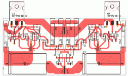
here shown without upper and lower gnd plane

my first pb , made with PC - ever !
Kicad proggie
for audiofanatic
it seems to me that distance from MOSFET to heatsink could be more than the length of the pins. Depends on the positions of PCB and heatsinks. Consider to move MOSFETS closer to the edge of the PCB.
Ladislav
it seems to me that distance from MOSFET to heatsink could be more than the length of the pins. Depends on the positions of PCB and heatsinks. Consider to move MOSFETS closer to the edge of the PCB.
Ladislav
If I may I ask... I don't see any decoupling caps in either the schematic or the photos of the amp...
Are they recommended for this topology... if so, is it a matter of bigger is better, or does there come a point where bigger just = smearing.
Are they recommended for this topology... if so, is it a matter of bigger is better, or does there come a point where bigger just = smearing.
Zen Mod said:
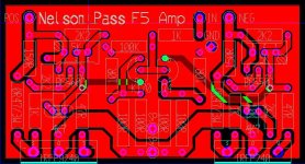
juma - is this good enough ?
here shown without upper and lower gnd plane
my first pb , made with PC - ever !
Kicad proggie
seems that I forgot attachment
Attachments
Zen Mod said:
juma - is this good enough ?
here shown without upper and lower gnd plane
my first pb , made with PC - ever !
Kicad proggie
Zen Mod said:
seems that I forgot attachment
Looks nice to me !
What is it ? 😉
juma said:
Looks nice to me !
What is it ? 😉
borbely/juma F5 intended gain stage 😉
Attachments
> borbely/juma F5 intended gain stage
Wrong thread !
http://www.diyaudio.com/forums/attachment.php?s=&postid=1555551&stamp=1215343219
😉
Patrick
Wrong thread !
http://www.diyaudio.com/forums/attachment.php?s=&postid=1555551&stamp=1215343219
😉
Patrick
EUVL said:>.......
Wrong thread !
.......
http://www.diyaudio.com/forums/showthread.php?postid=1565315#post1565315
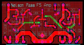
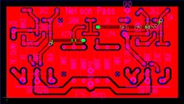
I dont think your pcb makes the requirement of the two 10r meeting at ground. Maybe it does and I am missing it.
Your left 10r and 100k meet but not at ground as in the schematic. I think you might need a ground trace running on bottom layer from 10r to 10r.
If I am wrong please burn me at the stake.
Uriah
Your left 10r and 100k meet but not at ground as in the schematic. I think you might need a ground trace running on bottom layer from 10r to 10r.
If I am wrong please burn me at the stake.
Uriah
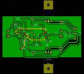
f5 pcb
Maybe the top SP connections are supposed to be the Speaker -, not sure, looks like a star or cross here. Doesnt ground at 10ohm ends like the AX schematic however as UDaily sayz.
Looks like the green traces are bottom side. I do like the layout.
udailey said:I dont think your pcb makes the requirement of the two 10r meeting at ground. Maybe it does and I am missing it.
Your left 10r and 100k meet but not at ground as in the schematic. I think you might need a ground trace running on bottom layer from 10r to 10r.
If I am wrong please burn me at the stake.
Uriah
Maybe the top SP connections are supposed to be the Speaker -, not sure, looks like a star or cross here. Doesnt ground at 10ohm ends like the AX schematic however as UDaily sayz.
Looks like the green traces are bottom side. I do like the layout.
- Home
- Amplifiers
- Pass Labs
- F5 power amplifier