Now I have the board powered up with light bulb and 10 turns to P1 and P2. R4 has 1.6V, R3 0 V
Does this mean jfet Q1 is blown?Now I have the board powered up with light bulb and 10 turns to P1 and P2. R4 has 1.6V, R3 0 V
hi acumos,Now I have the board powered up with light bulb and 10 turns to P1 and P2. R4 has 1.6V, R3 0 V
don't make adjustments with lightbulb in series
this procedure is just a security check for wrong connections/shorts
I know it, thanks. The problem is that after I blown the thermistor and changed mosfets I can't have voltage to R11. But I think that the problem is in the input jfet cause I dont' have voltage in any point.hi acumos,
don't make adjustments with lightbulb in series
this procedure is just a security check for wrong connections/shorts
ok zen, I have to use a jig like Borbely one...as previously - pull them (jfets) out and test them
same as or Idss testing
I know I'm a little dumb, but I'm trying to go better!
F5
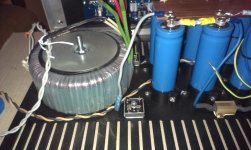
I have a problem my 50A bridges are in short circuit, I do`nt knew why, Any idea?
The amp worked for 5 to 6hours, i have biased the amp to 1,9A the borads are cascoded two pairs at 32+32VDC.
I have a problem my 50A bridges are in short circuit, I do`nt knew why, Any idea?
The amp worked for 5 to 6hours, i have biased the amp to 1,9A the borads are cascoded two pairs at 32+32VDC.
Attachments

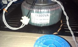

Caps are from apex jr should be ok. how to check them?
just check them with ohmmeter for short
if they're open circ (after some time , needed that ohmmeter feed them fully) , they're most probably good
Hi,
during initial testing I have 0.45 v across R11 and 0.30 v across R12,
0 volts DC at the output.
Why this difference between R11 and R12?
Thanks
during initial testing I have 0.45 v across R11 and 0.30 v across R12,
0 volts DC at the output.
Why this difference between R11 and R12?
Thanks
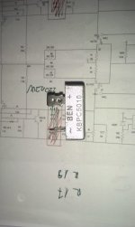
I found R11 & R12.
They are the output's Source resistors.
The current coming in through the top device MUST pass out through the bottom device and what little can pass along the NFB resistors.
The voltage differences you have measured are impossible if the Source Resistors are equal.
Did you match them?
Have you connected something else to the Output node?
R11 and R12 are both 0.47 ohm
I do not have anything connected to the output.
I will make other checks
I do not have anything connected to the output.
I will make other checks
R11 and R12 are both 0.47 ohm
Have you measured the actual resistance of each resistor? If there is a difference it will explain your measurements.
The good news is you can achieve that bias with zero DC offset.
Have you measured the actual resistance of each resistor? If there is a difference it will explain your measurements.
The good news is you can achieve that bias with zero DC offset.
Hard to believe one of them could be so far off, unless it's actually marked 0.33.
I completely agree, but you don't know until you measure. Each could be opposite ways off the marked value...
I completely agree, but you don't know until you measure. Each could be opposite ways off the marked value...
Maybe he's using 2 voltmeters, and one is off. If so, he could swap them and see if the low reading follows the meter.
- Home
- Amplifiers
- Pass Labs
- F5 power amplifier