Thank you MASantos, juma, BesPav, Andrew for your comments.
Here is what I have come up with.
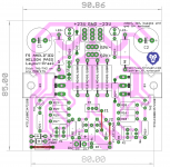
1. Bigger PCB to make mosfet mounting hole distance in line with UMS specs (80mm) (although xrk is dissipating 20-30 w from his class A amp without issues with 64mm spaced mosfets).
2. Fat a$$ traces
3. Compatibility with big fat Vishay RN60D resistors
4. options for
a) Zobel
b) Bypass caps for rail
c) LED (retained from previous layout)
d) Ground list (retained from previous layout)
these options are just that 'options'. only FAB (Fearless Amp Builders) could try.
the layout is very amenable to home etching with just 2 jumpers and min of 24mil clearances, except for pads of to-92, 3296W trimpot and led's. MOSFETs are mounted centrally and no requirement any PCB mounting holes (one less thing to worry).
Here is what I have come up with.
1. Bigger PCB to make mosfet mounting hole distance in line with UMS specs (80mm) (although xrk is dissipating 20-30 w from his class A amp without issues with 64mm spaced mosfets).
2. Fat a$$ traces
3. Compatibility with big fat Vishay RN60D resistors
4. options for
a) Zobel
b) Bypass caps for rail
c) LED (retained from previous layout)
d) Ground list (retained from previous layout)
these options are just that 'options'. only FAB (Fearless Amp Builders) could try.
the layout is very amenable to home etching with just 2 jumpers and min of 24mil clearances, except for pads of to-92, 3296W trimpot and led's. MOSFETs are mounted centrally and no requirement any PCB mounting holes (one less thing to worry).
Attachments
Last edited:

I can confirm that the layout Prasi did for me has no issues with hot spots at 20w per MOSFET. The use of the two MOSFET mounting screws to support the PCB works really well. It's very sturdy and convenient. If I wasn't making a headphone amp, I would have gone with UMS spacing as well.
Last edited:

You should mimic Nelson's long boards, with even spread of the heat on the sink. Those outputs become really hot so sink the heat properly!. I built mine (the very first DIY amp for me) with all of the components Nelson recomended, 6 years ago. It's been my daily driver and never even given me thoughts that it could blow-up!.
I one I posted above was Goffe's layout ( http://www.diyaudio.com/forums/pass-labs/121228-f5-power-amplifier-101.html#post1527301 -83mmx 35mm).
and check out here, this one looks the same layout. Nelson Pass F5 Take Five.. | Page 13 | Audiokarma Home Audio Stereo Discussion Forums
I feel, if one has big enough heatsinks, or is ready to use fan (low speed), 80mm should be sufficient distance.
However, I do agree that larger spacing would dissipate better, in that case my recommendation would be to go with diyastore PCBs.
Someone has built the F5 with the layout after all. I didn´t built this amp. One-side layouts are DIY friendly. I have done layout for BA-1 FE, BA-3 FE, BA-3B FE, X-ONO, UGS (Cheff design) and Sony VFET balanced FE. All one-sided no jumping wire and compact. I'll post it someday or send me a message.
Someone has built the F5 with the layout after all. I didn´t built this amp. One-side layouts are DIY friendly.
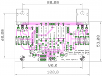
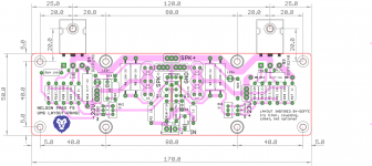
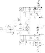
Thanks, yes I agree, one sided are diy friendly especially when PCB size exceeds 100mm. here is my version of UMS compatible layout based on popular demand.
I have included some optional components (coupling caps and i/p filter 🙄), which can be jumpered/omitted and the circuit can still be built as the original firstwatt article by Mr. Nelson Pass.
While making the layout I came across a small mistake in the F5 dimensions pdf document in the DIYA store documentaion (https://cdn.shopify.com/s/files/1/1006/5046/files/P-F5-1V20-dimensions.pdf)
The distance from PCB edge to MOSFET mounting hole is mentioned as 20mm, it should be 15mm. Store admins could take a look and take corrective action, although its not that important.
regards
Prasi
Attachments
here is my version of UMS compatible layout
Hi, Prasi!
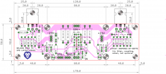
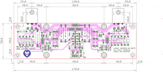
Just check, how and where load current will return?
If you provide such a layout, then SPK- wire must be connected straight to power ground on PSU capacitors.
But it would be better to provide local onboard decoupling caps, say at yellow marks, and create local power ground plane on the other side of the board.

Just imagine, all AC currents flows from one to another terminals of the nearest capacitor (with enough capacity and internal impedance). So all of them, both powerplanes, SPK+ and SPK- are better to place as near as possible and with big enough capacitors between powerplanes and SPK- as local powerground.
Here you can use top layer of the board as ground, this is the best possible decision. Proper way to eliminate ground loops in poweramps would be to divide PCB space to power and small-signal contours (as PWRC and SSC), and as a berry on a piece cake connect contours in just one place on PCB or provide different points to connect each of contour to amps Starground.

Better way to understand how poweramp are working is to imagine that this is definitely to discharge nearest capacitor to load and return load current to another terminal of that capacitor. That's all.
Hi, Prasi!
Just check, how and where load current will return?
If you provide such a layout, then SPK- wire must be connected straight to power ground on PSU capacitors.
But it would be better to provide local onboard decoupling caps, say at yellow marks, and create local power ground plane on the other side of the board.
An externally hosted image should be here but it was not working when we last tested it.
Just imagine, all AC currents flows from one to another terminals of the nearest capacitor (with enough capacity and internal impedance). So all of them, both powerplanes, SPK+ and SPK- are better to place as near as possible and with big enough capacitors between powerplanes and SPK- as local powerground.
Here you can use top layer of the board as ground, this is the best possible decision. Proper way to eliminate ground loops in poweramps would be to divide PCB space to power and small-signal contours (as PWRC and SSC), and as a berry on a piece cake connect contours in just one place on PCB or provide different points to connect each of contour to amps Starground.
Better way to understand how poweramp are working is to imagine that this is definitely to discharge nearest capacitor to load and return load current to another terminal of that capacitor. That's all.
Hi BesPav,
thanks for the comments, yes, i agree. my layout in post 21 follows all the guidelines and thats how i like it too.
here is a rough layout, which can still be improved.
reg
Prasi
Attachments
Last edited:
Hi BesPav,
thanks for the comments, yes, i agree. my layout in post 21 follows all the guidelines and thats how i like it too.
here is a rough layout, which can still be improved.
reg
Prasi
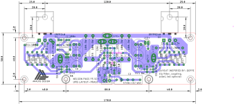
For the sake of completeness, here is the final version of the layout with decoupling caps as suggested by BesPav.
Reg
Prasi
Attachments
Nice layout, Prasi!
Unfortunately, home etching on cheap 75mm x 100mm boards won't work here. I need to find source of inexpensive long blank copper clad boards.
I agree. Nice. Single layer always makes things more difficult. The only thing I could say is that the inner PCB mountingv holes (on the mosfet side) are not necessary as the mosfets support the board well enough. Taking those out may help you spread things out a bit.
ok, i only have the latest version as per post #32 in my pc.
what i will do is replicate traces on top and remove inner mounting holes and post it here.
what i will do is replicate traces on top and remove inner mounting holes and post it here.
- Home
- Amplifiers
- Pass Labs
- F5 layout