Thanks Patrick, I'll think about it.
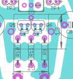
For matching, I am thinking about possibility to use this empty board and some kind of flat heat sink (peace of flat copper) with mechanical clip/clamp for SOT-23 without soldering.
I am not sure is it possible?
For matching, I am thinking about possibility to use this empty board and some kind of flat heat sink (peace of flat copper) with mechanical clip/clamp for SOT-23 without soldering.
I am not sure is it possible?
I managed to use the pads on the MEGA device tester to measure the parameters of sot23. The pads were not at the correct spacing, but it measured.
Using the pads of your PCB you could lay the sot23 on to them and apply a spring clip to hold it down and in place while you have meters and supplies attached to the other ends of the pads.
When you have them batched, you can then proceed to using both sets of pads to COMPARE one to the other measuring DIFFERENCE between DUT & REF.
I am thinking about using this heat sink for SOT-23 JFETs:
50pcs 13x13x11mm High Quality Aluminum Heat Sink for Chip Electronic H36 | eBay
Isolation sheet with window for JFETs will be needed & resistors go to the bottom layer.
For mounting I added to M2 holes (1.6 mm drill) distance center to center 15mm.
PS
Heat sink like this is additional ground shield for JFETs 😎
Attachments
Last edited:
I have not tested whether the 2Nxxxx JFETs are D-S swappable.
There is no reason why they are not, but you better check first, just to be safe.
LSJ74 has no SOT23 package, BTW. Only LSK170.
Patrick
There is no reason why they are not, but you better check first, just to be safe.
LSJ74 has no SOT23 package, BTW. Only LSK170.
Patrick
It seems to be general guidance that jFETS intended for RF duty are all D to S swappable. they are truly symmetrical.
But there does not seem to be similar confirmation that low frequency duty jFETs are equally symmetrical.
I have checked many jFETs (mostly lsk170, lsj74, 2sk170 & 2sj74) and swapping D & S does result in a very small difference of measured Idss. But this is a DC test, not at audio frequencies.
But there does not seem to be similar confirmation that low frequency duty jFETs are equally symmetrical.
I have checked many jFETs (mostly lsk170, lsj74, 2sk170 & 2sj74) and swapping D & S does result in a very small difference of measured Idss. But this is a DC test, not at audio frequencies.
We have curve traced ALL small signal JFETs we have in stock and can confirm they are swappable.
They include Toshiba, NXP, Sanyo, ......
We have not tested the 2Nxxx parts, nor the Jxxx parts.
Patrick
They include Toshiba, NXP, Sanyo, ......
We have not tested the 2Nxxx parts, nor the Jxxx parts.
Patrick
HI Patrick, yesterday I checked the datasheet for Fairchild JFETS 2N5457&2N5460 and this is citation:
NOTE: Source & Drain
are interchangeable
So, I hope all will be OK.
http://www.farnell.com/datasheets/46943.pdf
NOTE: Source & Drain
are interchangeable
So, I hope all will be OK.
http://www.farnell.com/datasheets/46943.pdf
LSJ74 has no SOT23 package, BTW. Only LSK170.
Patrick
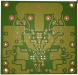
Board is compatible with both THT&SMD JFETs.
THT JPEGs can be both SGD&GSD with minimal bending.
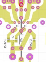
- added few test points (connector ready)
- added input filter C (SMD only)
- added alternate thermistor positions for easy mounting ( legs spreading friendly 😎)
- added alternate R7 for easy mounting (+ jumper wire)
Final?
- added input filter C (SMD only)
- added alternate thermistor positions for easy mounting ( legs spreading friendly 😎)
- added alternate R7 for easy mounting (+ jumper wire)
Final?
Attachments

Last edited:
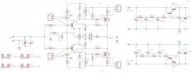
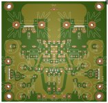
Could you change the power supply diagram so the V+ and V- point to the amp circuit and that the the RS1 and RS2 are the connection points for V+ and V- and you don't really need CM2/RM2 (and CM6/RM5) as you would have at least the basic ripple caps next to the rectifier diodes on the raw supply - Teddy Pardo did something like this on his 'Accelerated TeddyRegs', from memory (see his website or 'Pink Fish Media')
Are the CB1 and CB2 power rail filters? If so, should have their own separate ground connection, not lumped into the signal ground but not sure how significant this would be ...
If you use this h.amp to drive the less efficient planar 'phones, the output current and it's return are much more significant than usual headphones, so the ground return point will also be more significant and should be close to power supply output caps CM1 and CM5, not the signal ground point - this will require a major alteration in the design of the pcb (sorry for the late comments) but I think will be worth the trouble
Not sure about the double sided big fat track for the output signal - not really necessary - and a PIA to solder/change
What's R7.1 for?
I can, but what's the point, schematics is clear enough in my opinion.1.
Could you change the power supply diagram so the V+ and V- point to the amp circuit and that the the RS1 and RS2 are the connection points for V+ and V-
Cap Multiplier is EUVL's version, variation of standard circuit, I think it's good as is.2.
you don't really need CM2/RM2 (and CM6/RM5) as you would have at least the basic ripple caps next to the rectifier diodes on the raw supply - Teddy Pardo did something like this on his 'Accelerated TeddyRegs', from memory (see his website or 'Pink Fish Media')
Idea is to use little different biasing schema, or even experiment with different front end, but all this is optional, see3.
Are the CB1 and CB2 power rail filters? If so, should have their own separate ground connection, not lumped into the signal ground but not sure how significant this would be ...
http://www.diyaudio.com/forums/pass-labs/168040-f5-2sk2013-2sj313-5.html#post2285554
http://www.diyaudio.com/forums/pass-labs/210538-f5-bjt-input.html
I am not sure about about separate CB1+CB2 ground connection, I'll think about it.
PS
CB1+CB2 ground connection is unified with feedback ground connection via R7, but separated from pure input GND (connected on star only) so I think this is OK as is.
I'll answer later.4.
If you use this h.amp to drive the less efficient planar 'phones, the output current and it's return are much more significant than usual headphones, so the ground return point will also be more significant and should be close to power supply output caps CM1 and CM5, not the signal ground point - this will require a major alteration in the design of the pcb (sorry for the late comments) but I think will be worth the trouble
This is fast circuit, so I try to preserve speed. So very wide tracks on both sides, and no long close tracks with large delta V to minimize track induced inductance and capacitance in output&feedback area.5.
Not sure about the double sided big fat track for the output signal - not really necessary - and a PIA to solder/change
5.
What's R7.1 for?
Only one R7 will be mounted. R7 is very long horizontal mount, R7.1 is very short vertical mount. Mount one and short other.
Last edited:

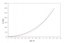
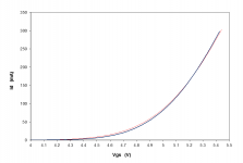
After finishing the first prototype, it is time to look into further optimisations.
What bothers me with the first prototype is that the IRF510/9510 I used were not a true complementary pair.
Amongst the 20 pairs I bought and matched, not a single N-P pair can be found even for Vgs match alone.
They differ on average by 0.3V at 150mA bias.
On top of that the Yfs are also not matched, as shown below. (~33% mismatch)
(Note that the Vgs of the N device in red has been shifted manually by 0.3V for better illustration of Yfs differences.)
Patrick
.
Attachments
Last edited:
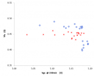
So I ordered another 20 pairs of FQP3N30/3P20 and curve traced them.
The results look much better.
If you pick the best N-P combination from all 40 devices, they are almost a perfect match.
The problems is that out of 40, I can only find one set of 4 devices which are this good.
Patrick
.
The results look much better.
If you pick the best N-P combination from all 40 devices, they are almost a perfect match.
The problems is that out of 40, I can only find one set of 4 devices which are this good.
Patrick
.
Attachments
Last edited:
The next figure shows the spread of both the Vgs and Yfs at 150mA bias.
As can be seen, the P device has a much larger spread of Yfs.
This might improve with a much larger matching pool than 20 pairs.
But the yield is not likely to improve dramatically unless one goes above 200~1000 pairs.
Patrick
.
As can be seen, the P device has a much larger spread of Yfs.
This might improve with a much larger matching pool than 20 pairs.
But the yield is not likely to improve dramatically unless one goes above 200~1000 pairs.
Patrick
.
Attachments
- Home
- Amplifiers
- Pass Labs
- F5 Headamp ?