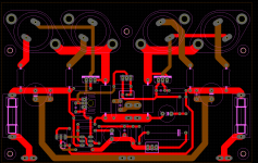
C2 is ~20mm away from the FET power pin.
That is at least 15mm too far.
Next you must bring the two decoupling caps very close to each other so that the total trace length from +FET (T2) to C1 to PGND to C2 to -FET (T1) is a short as possible.
This can only be done if the FETs are moved to near each other.
That is at least 15mm too far.
Next you must bring the two decoupling caps very close to each other so that the total trace length from +FET (T2) to C1 to PGND to C2 to -FET (T1) is a short as possible.
This can only be done if the FETs are moved to near each other.
C2 is ~20mm away from the FET power pin.
That is at least 15mm too far.
Next you must bring the two decoupling caps very close to each other so that the total trace length from +FET (T2) to C1 to PGND to C2 to -FET (T1) is a short as possible.
This can only be done if the FETs are moved to near each other.
In an ideal world that might be how it should be, but after looking at the original P3A layout it doesnt seem to matter much. Or Rod's original design is crap, which I sincerely doubt. 🙂
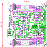
Took the previous version, rearranged a few components, added a 4.7uF cap again and switched from single to dual output pairs, for extreme situations when driving 4 Ohm loads and with enough power to drive atleast a resistive load down to 2 Ohm without trouble.
The amp PCB's have been ordered, now the waiting game begins.
Last edited:
Hmm, does it really matter that much?
But switching places with the 2 x 470uF electrolytes is easy enough.
Edit : Done.
Not my intention to sound negative, but why didn't you just use a single-sided pcb for this project?
As far as I see there's only one trace you would need a bypass-wire for.
Carlos
now with the recommended MJL4281A/MJL4302A output transistors.
C2 is ~20mm away from the FET power pin...........
..............This can only be done if the FETs are moved to near each other.
looks like I have gone way beyond "getting" confused.Where have the FETs come from Andrew? Are you getting confused 😀
I'll have a look in the garden for my brain, I'm fairly sure that's where I last remember it being.
Not my intention to sound negative, but why didn't you just use a single-sided pcb for this project?
As far as I see there's only one trace you would need a bypass-wire for.
Carlos
Well, firstly, some component placements was made easier and made for an overall cleaner layout. Secondly, the new version with dual output pairs needed a dual sided pcb anyway.
Besides, I'm getting them profesionally made so single or dual sided? Doesnt really matter.
Where I'm getting them made the price is the same, whether single or dual sided.
PCB's are on their way from China. Should be here sometime end of the week/early next week. I hope so anyway.
I would be really interested to know HOW you doubled the outputs. With CFPsit should not be as trivial as with EFs. Did you double the drivers as well? Did you add emitter resistors on the power devices? Did you put base stoppers? Just some question that arise...PCB's are on their way from China. Should be here sometime end of the week/early next week. I hope so anyway.
Bye
effebi
I have already received my first PCB's, however Im already considering other options, like a P3A with 2 x pairs of TO-3 transistors.
Like the attached picture.
Ill most likely use my current PCB's but one can always consider future versions. 🙂
Like the attached picture.
Ill most likely use my current PCB's but one can always consider future versions. 🙂
Attachments
Last edited:
I would be really interested to know HOW you doubled the outputs. With CFPsit should not be as trivial as with EFs. Did you double the drivers as well? Did you add emitter resistors on the power devices? Did you put base stoppers? Just some question that arise...
Bye
effebi
Emitter resistors, yes, they have been added.
It is done as recommended by the designer, Rod Elliott.
This and the other P3A threads are good tutorials for newbe PCB designers.
I saved all the PCB diagrams to my computer for careful study of the evolution of the design. I only wish the PCBs are numbered serially, R1, R2, ... etc for ease.
Finally, dear neutrality, how does your design sound?
I saved all the PCB diagrams to my computer for careful study of the evolution of the design. I only wish the PCBs are numbered serially, R1, R2, ... etc for ease.
Finally, dear neutrality, how does your design sound?
What about mod in the original schematic to current mirror load on LTP and current source replacing led and Tr (as in p101). Any prediction of improvement in stability?
Nice layout ,but not diy friendly .
Regards,Alex
Thanks Alex mm, I am learning from your excellent examples. 'not-diy friendly' because double sided?. or due to something else?
regards
Prasi
have you a diy friendly pcb for this amplifier?Nice layout ,but not diy friendly .
Regards,Alex
Last edited:
Thanks Alex mm, I am learning from your excellent examples. 'not-diy friendly' because double sided?. or due to something else?
regards
Prasi
I guess "one sided" is DIY friendly, P3A is a small circuit, uses very few parts. You can make a very compact one sided through hole PCB out of it.
hi all,
i have made a layout for ESP P3 (not P3A), trying to minimize the size with mostly through hole components. the smd cap is optional as per the ESP website.
pl remove this post if this is not allowed.😀
prasi
what is P3?
the above link doesnt seem to be working... here is the link again.
High Quality 60 Watt Power Amplifier
....
- Status
- Not open for further replies.
- Home
- Amplifiers
- Solid State
- ESP P3A