Hi
I'm building my first DAC using a ESS ES9038Q2M DAC in voltage mode. The outputs (balanced XLR) will be fed into a pair of KRK monitor speakers. My area of expertise is more in the digital side of things, so I was hoping someone can help me the basics of blocking the DC bias of the DAC.
In voltage mode, the DAC will output the differential voltage with an offset of 1.65V (3.3V AVVC / 2). Ideally I would like to filter out the DC bias but I'm not sure of the series capacitor value and if a resistor should be added to ground? The monitors specify 5.12KOhm balanced input impedance.
There is an existing thread mostly dedicated to that dac chip. ES9038Q2M Board
Used to be some advice available from the ESS downloads page, but looks like they have password protected it. Downloads – ESS Technology, Inc.
Copy of old download attached.
One thing to possibly note: Distortion is much higher in voltage mode as compared to current mode. Some people including me find voltage mode distortion unlistenable.
Attachments
Your monitor speakers should be able to deal with the common mode DC offset of 1.65V just fine. Moreover your monitor speakers will most likely have DC input blocker caps in the input stage already. Might want to check this out beforehand.
If you want to implement DC blocking yourself you can calculate the cap's value as:
C = 1 / (2 * pi * f * R)
f is the desired cutoff frequency where the response is 3dB down. I'd suggest something between 1Hz and 10Hz.
R in your case is 5.12k/2 = 2.56k as each leg of the differential line sees only half the differential input impedance.
A practical example:
C = 1 / (2 * 3.14 * 2.56kOhm * 10Hz) = 6.2uF
It's good practice to use 100k resistors after each DC blocking cap to ground to discharge the output terminals to ground level even if nothing is connected to the output.
There is an existing thread mostly dedicated to that dac chip. ES9038Q2M Board
Used to be some advice available from the ESS downloads page, but looks like they have password protected it. Downloads – ESS Technology, Inc.
Copy of old download attached.
One thing to possibly note: Distortion is much higher in voltage mode as compared to current mode. Some people including me find voltage mode distortion unlistenable.
Thanks for the application note! Yeah I'm leaving solder bridges on the board to later add a daughterboard with a proper I/V stage. For right now, I've designed the daughterboard according to ESS's reference evaluation board schematic, but the op-amps they ure are out of stock everywhere. And given the cost of adding a output stage, I rather want to familiarize myself a bit more with analog electronics.
Out of interest, I found an article talking about the Sabre DAC's in voltage mode vs current mode.
Part 1 https://hifiduino.wordpress.com/2012/12/14/how-good-is-es9018-in-voltage-mode/
Part 2: https://hifiduino.wordpress.com/2013/07/15/how-good-is-es9018-in-voltage-mode-part-ii/
I'm keen to compare the differences, but it seems like the chip shortage is going to last a while.
Your monitor speakers should be able to deal with the common mode DC offset of 1.65V just fine. Moreover your monitor speakers will most likely have DC input blocker caps in the input stage already. Might want to check this out beforehand.
If you want to implement DC blocking yourself you can calculate the cap's value as:
C = 1 / (2 * pi * f * R)
f is the desired cutoff frequency where the response is 3dB down. I'd suggest something between 1Hz and 10Hz.
R in your case is 5.12k/2 = 2.56k as each leg of the differential line sees only half the differential input impedance.
A practical example:
C = 1 / (2 * 3.14 * 2.56kOhm * 10Hz) = 6.2uF
It's good practice to use 100k resistors after each DC blocking cap to ground to discharge the output terminals to ground level even if nothing is connected to the output.
Awesome, thanks yeah, I actually sitting with my function generator on my desk now trying to simulate different scenarios. Just wanted to check also, I'm planning on using C0G SMD capacitors for this on the actual PCB, but for now I only have some through-hole electrolytics which are polarized. I assume the negative pin of the cap is on the XLR connector side (and the positive on the DAC side)?
I do believe the speakers amplifier should probably have DC blocking on the input stage, but at the very least I want to leave footprints on the board just in case.
ESS originally used AD797 opamps, but later switched to OPA1612. Some people like to use OPA1656. There is an output stage project and an AVCC power supply project in the other thread. Schematics for both are attached to post #3003.
If using electrolytics for DC blocking, you might try Panasonic FM, say, maybe 470uf (I kind of prefer the sound of that value verses higher or lower for some unknown reason), in parallel with, say, maybe .1uf Wima FKP2. It may take some time for the cap sound to settle in, but the dac likely has so many other distortion and jitter problems the cap sound may not be noticeable.
Positive end of the caps go towards the dac chip. If you implement opamp I/V at some point, and depending on feeback resistor value and resulting voltage swing, it could be possible to reverse bias electrolytic caps if still used for DC blocking. While reverse biased they will conduct more or less similar to a diode and introduce additional distortion.
Last edited:
@recre8: Yes, positive terminal of the cap goes to the DAC output as it has the more positive voltage (+1.65V) compared to ground (0V). If you actually plan to use C0Gs that doesnt matter as they are not polarized. High valued C0Gs (IME >100nF) is not cheap though!
@Markw4: You do realize that you never answered any question the OP had?
@Markw4: You do realize that you never answered any question the OP had?
Thanks for all the help guys. Really appreciate it. I'm looking forward to comparing voltage out to current out with a proper I/V stage. Biggest problem for me with an IV stage is the need to get proper negative voltages so the footprint increases quite a bit (PCB transformer, rectifier, positive and negative regulators etc). But if it makes a big discernable difference, I like the idea of playing around with different op-amps.
I would rethink using NP0/C0G for DC blocking. To get the values you probably want/need, you will have to buy them in stacked assemblies (very expensive) or solder multiple MLCCs right next to as well as directly on top of each other (not a good idea for a multitude of reasons imo). Maybe just keep using electrolytic capacitors and consider using a footprint that can take both SMD and through-hole caps.
Creating a split supply for a potential I/V stage is not a big deal. You can use small DC/DC converters and put LDOs behind them or rely on passive filtering and OpAmp PSRR. It can probably be done on one square inch of PCB if you are willing to use 0402 SMDs. No need for PCB transformers. You can take a look at the schematics of the original Khadas Toneboard, they used Ricoh R1286 for this purpose. There are many other options but I don't remember all the part numbers. Depending on I/V stage gain, maybe even LM27762 is an option.
@Tfive: I think your remark against Markw4 is absolutely unasked for and I don't see why you are trying to pick a fight here. Not everything he posted was explicitly asked for, but he provided valuable information nonetheless.
You do realize that you never answered any question the OP had?
You already did it okay in terms of theory. I find there is more to the sound than simple corner frequency modeling predicts. Also, whether or not there is a resistor to ground is often seen as optional (not a bad idea though).
I would rethink using NP0/C0G for DC blocking. To get the values you probably want/need, you will have to buy them in stacked assemblies (very expensive) or solder multiple MLCCs right next to as well as directly on top of each other (not a good idea for a multitude of reasons imo). Maybe just keep using electrolytic capacitors and consider using a footprint that can take both SMD and through-hole caps.
Creating a split supply for a potential I/V stage is not a big deal. You can use small DC/DC converters and put LDOs behind them or rely on passive filtering and OpAmp PSRR. It can probably be done on one square inch of PCB if you are willing to use 0402 SMDs. No need for PCB transformers. You can take a look at the schematics of the original Khadas Toneboard, they used Ricoh R1286 for this purpose. There are many other options but I don't remember all the part numbers. Depending on I/V stage gain, maybe even LM27762 is an option.
@Tfive: I think your remark against Markw4 is absolutely unasked for and I don't see why you are trying to pick a fight here. Not everything he posted was explicitly asked for, but he provided valuable information nonetheless.
Thanks for the recommendation of the Khadas board. I checked the schematic and it's definitely a better solution for my case compared to a linear power supply. After checking the schematic for the khadas, it reminded me of a question I never really figured out: Why do so many of the DAC designs supply the op-amp with +/-12 or even 15V when the output range is only about 4vpp? Most of the audio op-amp datasheets I've looked up so far have pretty decent common-mode voltage range, so is it really necessary for such a wide supply range?
There is a lot of RF mixed in with the audio coming out of the dac chip. The opamps appear to be most tolerant to that at a particular power pin voltage. For Topping D90, an AK4499 dac, they used +-11v for the opamps. I did my own tests to find out why. That was where audible distortion turned out to be lowest.
I'm making progress on the design of my I/V stage. I had to pick and choose from the parts thare are currently in stock (which is slim pickings tbh) but so far I have:
LT3471 Boost/Inverter to get +18V and -18V.
TPS7A49 Positive LDO for +18V to +15V
TPS7A30 Negative LDO for -18V to -15V
OPA1612 Dual op-amps
But I'm struggling with a few of the key concepts.
1. Opamp feedback resistor - In the Sabre reference design and application note, the feedback resistor is 2.72K, whereas in most other examples the resistor is around 800 ohm. The 2.72K seems very high and when I model it as such, the output is about 7V peak to peak. With 820 ohm, the output is about 2.25Vp-p. 7V seems very high for line output, even for professional level?
2. The sabre reference design puts a AVCC(3.3V) voltage divider of 10K and 6.34K on the non-inverting input of the op-amp (1.283V) whereas most other designs divide it equally (1.65V). Why the one-third divider as opposed to equal divider?
3 Both biasing options in Question 2 result in the output being offset from circuit ground. What would happen if we simply gave circuit ground to the non-inverting input? Then the waveform would have no DC offset? What are the drawbacks?
3. With regards to the DC offset relative to circuit ground: I don't fully understand balanced audio: Is the ground wire in a balanced audio cable used for anything other than shielding? Meaning if there is a DC offset on Hot and Cold relative to the cable shield/ground, does it matter? Or does the device that takes the balanced audio in create it's own virtual ground?
I'm attaching
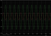
- my simulation schematic and the results, with green being the sabre reference design (2720 ohm feedback) and red being most other designs (820 ohm feedback)
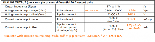
- The analog ouput section of the ES9038Q2M datasheet with my calculated values
- The ESS reference design document I keep mentioning.
LT3471 Boost/Inverter to get +18V and -18V.
TPS7A49 Positive LDO for +18V to +15V
TPS7A30 Negative LDO for -18V to -15V
OPA1612 Dual op-amps
But I'm struggling with a few of the key concepts.
1. Opamp feedback resistor - In the Sabre reference design and application note, the feedback resistor is 2.72K, whereas in most other examples the resistor is around 800 ohm. The 2.72K seems very high and when I model it as such, the output is about 7V peak to peak. With 820 ohm, the output is about 2.25Vp-p. 7V seems very high for line output, even for professional level?
2. The sabre reference design puts a AVCC(3.3V) voltage divider of 10K and 6.34K on the non-inverting input of the op-amp (1.283V) whereas most other designs divide it equally (1.65V). Why the one-third divider as opposed to equal divider?
3 Both biasing options in Question 2 result in the output being offset from circuit ground. What would happen if we simply gave circuit ground to the non-inverting input? Then the waveform would have no DC offset? What are the drawbacks?
3. With regards to the DC offset relative to circuit ground: I don't fully understand balanced audio: Is the ground wire in a balanced audio cable used for anything other than shielding? Meaning if there is a DC offset on Hot and Cold relative to the cable shield/ground, does it matter? Or does the device that takes the balanced audio in create it's own virtual ground?
I'm attaching
- my simulation schematic and the results, with green being the sabre reference design (2720 ohm feedback) and red being most other designs (820 ohm feedback)
- The analog ouput section of the ES9038Q2M datasheet with my calculated values
- The ESS reference design document I keep mentioning.
Attachments
1. Opamp feedback resistor...
It can affect more than just output voltage. Other things that may be affected include hump distortion, and or other harmonic distortion, and or sensitivity to RF from the dac in terms of whether or not the opamp might try to exceed its slewing capability. Suggest using a combination of measuring and listening to help understand any tradeoffs there may be.
2. The sabre reference design puts a AVCC(3.3V) voltage divider of 10K and 6.34K...
Sometimes lowering the reference voltage helps with hump distortion.
3 Both biasing options in Question 2 result in the output being offset from circuit ground...
One can remove DC offset from the I/V output by appropriate selection of the non-inverting input voltage divider. One may or may not find that dac sounds as good when the opamp is biased that way. Since pots can add distortion, a pot could be used to find the desired division ratio, then the pot could be replaced with fixed resistors before judging distortion results.
3. With regards to the DC offset relative to circuit ground: I don't fully understand balanced audio...
Pin 1 Revisited
https://www.hypex.nl/img/upload/doc/an_wp/WP_The_G_word.pdf
- Home
- Source & Line
- Digital Line Level
- ES9038Q2M Voltage Mode DC Blocking