I am just talking about clocks/oscillators. There's plenty of discussion about this elsewhere (I've already mentioned one place to start), so I'm not going to go on about it.
congrats with new object for audio investigations!
mine was working instantly. in fact the IR receiver board responds also to Onkyo remote, erratic though. anyway, what pairing can be done with an IR remote?
Dead battery in a brand new Apple Remote. Will need to go to Walmart to pick up some fresh CR2032. Hope that it should work.According to the seller's auction post, the Apple Remote has many modes. Hold the menu and big circle bottom for 6 seconds while pointing to the IR receiver should pair them. I may have to try several times before it works according to the seller. Wish me luck.
I may also need a flesh battery, but do not have one on hand.
I understand. I am unlikely to touch any SMD on my board. Mine was just a curious question on how clocks/oscillators should be specified for DAC application.I am just talking about clocks/oscillators. There's plenty of discussion about this elsewhere (I've already mentioned one place to start), so I'm not going to go on about it.
I will be very interested in measuring the noise floor spectrum of the board as is too. But it is probably out of my league.
Was just looking at LT3045 datasheet. Interesting. It sounds like to get full performance it needs attention to all the little details similar the DAC chip itself. In particular, it seems that LT3045 and LT3042 are especially sensitive to stray magnet coupling. That, and because to get down to -120dB level performance all the little details matter even if it is a voltage regulator instead of a DAC.
Actually the LT3045 datasheet doesn't say that it's especially sensitive to magnetic coupling. It talks about minimizing pick-up of magnetic fields if following a switching converter. All regulators have the potential to be affected by such pick-up if laid out poorly, and high performance parts will show any problems more clearly, so the datasheet gives recommendations to avoid this.
If the module designers did the same quality job awith the regulator modules as with Chinese DAC boards, maybe no wonder people haven't seen sound quality perhaps as good as anticipated and perhaps as good as the ESS op amp circuit. Don't know of course, but for it to be a fair comparison one might need to read the LT3045 application notes carefully and also read the "DEMO MANUAL DC2491A" demo board manual, which is recommended to read in the LT3045 application notes.
Many people have had great results with the LT3045. Modules can be bought from other countries such as Germany and the USA, or people can build them themselves as you are encouraging them to do with the op-amp solution. Of course, correct layout is every bit as important with op-amps, as you’ve found with your overheating output stage.
So, before I go off and do a lot of reading, has anybody else studied the documentation carefully and followed all the recommendations to get full -120dB rated LT3045 performance? If it has been tested carefully for AVCC supply use with attention to small details and DAC sound quality is not good enough then no need for me to repeat the experiment.
So, after telling people to think like engineers, you are willing to take one subjective report against the part over objective data, and despite the many subjective reports in it's favour. Why are you trying so hard to discredit an alternative approach to getting great results?
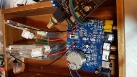
My lifepo4 battery powered es9038q2m board. One for oscillator and dual pack for rest.
I have removed most of the unused caps and replace those near dac.
Output is Jensen jt11 10k with 680ohm across +- dac out pins.
Testing one channel for now and sound very good.
I have removed most of the unused caps and replace those near dac.
Output is Jensen jt11 10k with 680ohm across +- dac out pins.
Testing one channel for now and sound very good.
Attachments
@Spartacus,
To begin with I did not say I read all the LT3045 applications information carefully, in fact I think I made it clear that i did not. I asked if anybody else did and if they made sure they were using them in way likely to produce the performance that people seem to point to when they express interest in using the devices. So far, nobody has responded that they did.
At this point we don't know anything at all about how well some of the Chinese LT3045 modules actually perform as compared to the best performance possible shown on the first page of the data sheet.
In addition, I isn't clear if anybody has used particular Chinese LT3045 regulators to produce a modded ES9038Q2M DAC that with the -120dB distortion specs ESS claims. If anyone has, please post your results. Or, at least please post whatever you have found.
Now I would like to change the perspective of my comments as follows:
There seem to be a wide variety of people interested in the low-cost ES9038Q2M DAC boards. The concerns I have expressed are mostly directed towards people who want to make a DAC that is as good as possible out of the one we are starting with.
There are other people who may just want to play around and experiment to have fun. And there are people with varying degrees of expertise and experience. Some people are equipped to measure results or have a reference DAC to compare with, or ideally, some combination of both.
For somebody who knows what they are doing and how to measure their results I have no problem whatsoever with whatever they want to do. Same for people who just want to play around and see how they like the sound.
For people who want to make the best DAC they can and who want to have a known way that has already been shown to work, I have described a way of doing it that leveraged research and recommendations made by ESS, the manufacturer of the ES9038Q2M DAC chip. It works. I don't want that particular group of people to be excited into playing around with mod approaches where we cannot say if you do it this way it should work because we know this one did, along with pictures on advice on how to do it.
Once more I would like to change the subject:
I have not reported on further progress yet, but minimal size stick-on heat sinks attached to the LME49720 opamps is keeping them comfortably cool.
I mentioned a concern about possibly RF oscillations or RF pick up from another area of the DAC board that I wanted to check into as possible causes of heating. I was voicing concerns about about my biggest worries. There were always more benign possibilities. It could be that the temperature of the opamps is related in some part to very compact construction of the modded board, for example.
In the interests of full disclosure, recent environmental measurements show something rather unique about the RFI/EMI environment here that is not likely be the case for anyone else. I am located on top of a hill. On a very clear day I can see about 100 miles across the Sacramento valley to the Coastal Mountain range. Over the next hill from me is a small airport. Out in the valley in front of me is an international airport and an Air Force base. Not too surprising there is radar being used in the vicinity, and some of it appears to be operating at around 130MHz-150MHz range. Sitting out in the open, my Chinese DAC board and all my other equipment are in a fairly strong pulsed RF field. Enough to produce some spurs I can see in the ES9038Q2M output that did not appear in the much quieter EMI/RFI environment at Richard Marsh's. The spurs are down around -110dB, but considering that LME49720 opamps are known to be sensitive to DECT phones and other RF sources, probably not surprising (in fact there is a DECT phone here with the base station about 10 feet from the DAC board, and the base station needs to be turned off when I work or it produces somewhat bigger spurs than the radar). One possibility is that the radar band RF exposure is causing some temperature rise.
I have tried various approaches at shielding that have not been effective. I am thinking of options including moving some of my work to another location across town. Since the radar discovery is relatively recent I can't quite say yet if the case is closed on the mystery of opamp temperature.
Eventually, the issue should be moot once the DAC is put in a closed steel case. However, at that point it would be much more difficult to experiment with and before I can design it into a case I need to finalize the power supply design and get it off my linear bench supply.
Bottom line: other than the compact layout of the mods, whatever heat there is in the opamps my have nothing to do with anything I did or could have done to prevent it. At this point it seems highly likely that is the case.
In the meantime maybe better to not assume too much (and I am not), and rather wait with some patience to see how things turn out after some more time has gone by and more work has been done.
Last edited:
I see some uses 80mhz instead of 100mhz for the es9038. Does 80mhz give better jitter spec than 100mhz?
Also, I assume my board uses async mode, is there a way to convert it to syn mode?
Also, I assume my board uses async mode, is there a way to convert it to syn mode?
Probably only slightly. Within the same model clocks differing only in frequency, the lower frequency clocks tend to have lower jitter. To get more of a difference than that one would typically need to go to a different model clock that is designed for less jitter. For the NDK clocks, for example, the ultra-low jitter models are only available below 50MHz.Does 80mhz give better jitter spec than 100mhz?
Also, I assume my board uses async mode, is there a way to convert it to syn mode?
Yes. But its about as hard as the hardest mods. There are two basic synchronous modes, master and slave. Slave is easier, but might tend to give more jitter. Master is harder to do. For an ES9038Q2M like this one you might want to sign a nondisclosure agreements with ESS and get a copy of the data sheet. Unless you are pretty knowledgeable you probably wouldn't understand it, but at least other people could talk to you in private about how to do it. It would involve connecting up an external microcontroller to reprogram the Q2M registers, including some hardware mods to make that possible and perhaps a mod to be able to export the master clock signal.
In addition, if you wanted to use 128_fs master mode where the Q2M controls the I2S serial interface clocks then you would need to choose a clock frequency carefully because you would have to decide which PCM modes you wanted to support. You can choose either the 44.1k series or the 48k series (well, you would have to choose unless maybe if you wanted to use external ASRC).
For slave mode with ASRC disabled (128_fs mode), IIRC, the Q2M would be using the external clock in your I2S master device. Have to be careful about doing it that way because jitter can get worse if the interface is noisy or if the I2S master has other than an ultra-low jitter clock.
If you think you might be interested but want to know more, I posted some pictures of how to hook up an external microcontroller while preserving the original one on the board.
EDIT: By the way, synchronous mode gets a lot of attention but I'm not sure why. Some of the best (world-class, actually) DACs around use ASRC including Benchmark and Crane Song. There is no fundamental reason why ASRC should sound bad. If sometimes people find that turning off ASRC sounds better then somebody should figure out why because that shouldn't be.
Last edited:
Hi all,
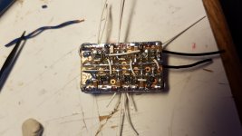
today I finished my new add-on board for i/v conversion and AVCC opamp stage. I choose same values as Mark (820R//220pF) and modified the existing on board differential circuit with thin film resistors and COG caps. The supplier wanted to test me and sent 0603 size caps - but with some copper film I could connect even these 4 tiny chips.
After first trial I was shocked - a big bang came out of my speakers and I thought that was it... I then shielded the i2s wired and checked all connections again. I placed a carton stripe between add-on board and DAC-board as I was afraid some solder points of the on board opamp connected through the isolation tape I already placed and connected some paths with the new add on board - and I guess this did it. No cracks anymore, no bang, but a stable sound coming out of my system now - and what a sound! Sound appears warmer now with more deep bass volume, a little as if AVCC caps were increased. But all that with a smoother and finer structure, that makes the sound more natural. At the same time it has more dynamic and I am more willed to turn up the volume - usually a sign for less distortion. I am quite happy with the result.
After a longer listening session I checked the temp. of the opamps and yes they were quite hot. No idea where this comes from - could it be the value of 820R and 220pF that you also use Mark? My 9028q2m board opamps stay quite cool with nearly the same design, but 330R//100pF for i/v stage, inverted differential stage (DACB line goes to inverted differential opamp entry while on ess circuit it is the DAC path) and no AVCC opamp stage.
Seems I also have to look for a cooling solution now...
Thanks to Mark for your big motivation here that lead me to the best sound I heard so far over my home system!
Attachments
Last edited:
freezebox, Great news! Good to see you make some progress. I agree that as the sound becomes more natural with less distortion it actually sounds better, but unless people hear it for themselves it can be hard to imagine what it is like.
Also, it was amazing to me at first when I found I could solder little SMD parts. Didn't think I was going to be able to do it before I tried it. Interesting how that works.
What I did to cool the opamps was cut off about a third of a heat sink and used the bigger 2/3s piece for the opamp: Amazon.com: Aavid Thermalloy 501200B00 Heatsink, Passive, DIP 14/DIP 16, Straight, Extruded Epoxy, 0.73" L x 0.25" W x 0.19" H, Black (Pack of 10): Industrial & Scientific
Stuck the heatsink onto the top of the opamp with some thermal tape like this: Amazon.com: Thermal Adhesive Tape (20mmx25 Meters 0.1mm thickness) Nicelux Double Side Adhesive Thermal Conductive Tape for Heat Sink of LED Light, PC and More, Electrically Insulated,1 Reel Pack: Computers & Accessories
EDIT: Maybe its getting around the time to start thinking about a clock upgrade? You will like the improvement with that if you like what you have so far, IMHO.
Last edited:
freezebox, Also, I don't think the passive component values cause the heating. If anything it is likely a little low level RF that makes its way out the analog outputs. Maybe that's why ESS recommended circuit has so much filtering, to try to get rid of as much of that as possible before the analog signals leave the DAC board.
In addition, the LME49720 data sheet says the opamps can run at up to 85 degrees C. That's pretty hot, 185 degrees F, too hot to hold your finger on. Personally, I feel more comfortable with the heat sinks.
In addition, the LME49720 data sheet says the opamps can run at up to 85 degrees C. That's pretty hot, 185 degrees F, too hot to hold your finger on. Personally, I feel more comfortable with the heat sinks.
Last edited:
I have already sticked some heatsinks you can buy for Raspi PCU. They are adhessive and the small one fits perfectly to opamp, but probably too small for the power which is dissipated.
I was also happy and surprised, how good it worked to solder the small smd parts.
Waiting for my NDK clock to arrive..
Any further idea what could be the reason of this hot opamps? Could the analog ground be separeted from digital ground as most of us modders use at least 2 different PSU for analog and digital anyway?
Last edited:
Any further idea what could be the reason of this hot opamps?
I don't think the heating is related to the power supply or ground. For one thing, my AVCC LME49720 opamps run slightly warm, but much cooler than the same LME49720 opamps used in the output stages and connected to the same power. In addition, I did some experiments with moving around power ground returns without seeing any measurable changes in anything. Nothing audible changed either.
The only explanation I can think for us to both see the same heating effect would be some low-level rf coming out of the dac outputs that go into the IV opamps, as I said. There probably is some, only a question of how much and what does it usually do to LME49720 opamps. ESS would not have needed to add all the low pass filtering if there wasn't some RF to attenuate.
As long as you have the 33pf caps on the differential stage and some little heat sinks to make your finger feel better when you touch the opamps I don't think there is anything else to do at this point. Also, because SQ is good, and my DAC measured quite well at Richard Marsh's, and also because the opamps are rated to run at up to 85C, I don't think there is reason to worry at this point. In addition, since ESS recommends LME49720 opamps, and assuming some heating is normal, chances are ESS doesn't have much concern about a little heat well within the opamp specs either.
That being said, I will keep an eye on it and see if anyone else reports any different circuit behavior. If one turns up that runs cool, that would certainly be reason to investigate further. Probably not going to happen though, seems most likely the heat is normal for those particular opamps in this application.
Only concern is we might not want to take chances that we might heat up anything in a big downstream power amp. That could be good reason to favor use of the recommended ESS differential stage circuit with all the filtering for the single-ended outputs. That would be true regardless of the particular ESS recommended (or other) opamps chosen for use in DAC output stage mods.
Last edited:
The 9028q2m board with I/V stage I have has a quite similar circuit as I currently have. My current schematic is shown below. They use 2x 4k7 for voltage devider for offset voltage and use 330R//100pf in I/V stage. The opamps do not run hot on this board. It has a seperate ground plane for digital parts as far as I can judge it. The reason why I did not implement the ess recommended circuit was, that the feedback resistor in I/V stage is very huge and I was not sure for which DAC chip this was designed. As 9038q2m has double inner resistance as 9028 and on my 9028 board they use 330 Ohm, 820 seemed reasonable to me.
But probably it is the 9038q2m chip that produces some RF noise and 9028q2m does not...
But probably it is the 9038q2m chip that produces some RF noise and 9028q2m does not...
Attachments

Last edited:
The reason why I did not implement the ess recommended circuit was, that the feedback resistor in I/V stage is very huge and I was not sure for which DAC chip this was designed.
Regarding the feedback resistor for the IV stage, it depends on the DAC chip (and depending on chosen AVCC supply voltage) for the maximum output current it can produce. If the opamp is able to source or sink that much current, then the resistor just determines how far the opamp output voltage will have to swing up or down at full current. If it is within the output voltage range of the opamp then it should work.
Resistor size also affects noise produced in the first stage which usually sets the noise performance for the rest of a circuit. Once noise in the audio band is there it will pretty much be there forever. The resistor also affects voltage output of the first stage. Depending on the opamp, distortion may vary with output voltage swing so the resistor could have some effect on distortion performance.
The resistor and cap in parallel with it form a low pass filter with a corner frequency at 1/(2pi*RC). The first thing that gets affected in the audio band depending on the chosen corner frequency is phase shift at 20kHz. Setting the corner frequency at, say, 50kHz might cause audible phase shift at lower, audible audio frequencies, so the corner frequency is usually set at maybe a few hundred kHz for Hi-Fi purposes.
Regarding opamp heating, hard to say how much 9028Q2M vs 9038Q2M affects that, and how much ground plane(s) design affects that. Both things could potentially have some effect. While separate ground planes would be great, we are stuck with the combined ground plane for this DAC board. Despite that, it is possible to get good distortion numbers with some care doing mods.
Last edited:
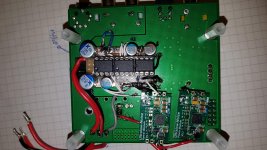
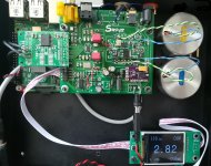
Today first test ... very good. This is for now, back to another work.
No problems with opamp stages 🙂. I have set it to 5Vpp because i drive poweramp dirrectly, nice clean output, noise lower than with opamp stage. Cant measure THD and SNR. But scope shows no anomalies, that i saw at a lot of other designes.
No problems with opamp stages 🙂. I have set it to 5Vpp because i drive poweramp dirrectly, nice clean output, noise lower than with opamp stage. Cant measure THD and SNR. But scope shows no anomalies, that i saw at a lot of other designes.
Attachments
Mark4
You did change the clock oscillator...is under the clock soldering mask (place) also for smaller clocks? Or are pins just for clock in same dimension?
Thank you.
You did change the clock oscillator...is under the clock soldering mask (place) also for smaller clocks? Or are pins just for clock in same dimension?
Thank you.
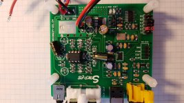
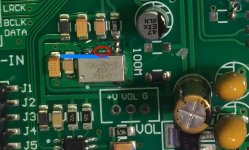
There is one unused set of solder pads under the clock for a slightly smaller clock, or for a clock with the pads in a different location. One of the other pads is shown in the pic below circled in red. The trace that connects it under the clock is shown in blue.
There is one more pad below the red pad (towards the bottom side of the picture), underneath my new clock about half way across from left to right, like the one I circled on the top side of the picture. It also has a trace that extends to the pad on the left of it, or in the left direction as shown in the picture view.
Also, in the picture it can be seen where I cut back the ground plane a little bit around the clock pads I used for the new clock. The reason I did that was because the new clock I used was a little bigger than the old one, and I wanted some more clearance around the pads for soldering in the new one. I used a sharp point Exacto knife to cut and then peel way a little bit of the ground plane as shown. Didn't want to cut too much though, so was very careful to try to get a suitable amount.
To remove the old clock I first un-soldered the volume header to make some room for my solder iron in the area around around the clock. I found the minimum temperature to set my solder iron to melt the original solder on the board and then set my iron a bit hotter than that to be sure the original solder would melt without using any extra, unneeded heat. I tried to solder wick off some of the original solder without much luck.
Then I added Chip Quik solder remover alloy to the pins with enough heat to melt the original solder in order so as to dilute and mix in the Chip Quik with the original solder. I had a big ball of Chip Quik added on each of three of the clock pins and was starting to add it to the fourth pin when the clock suddenly just fell off. Sometimes that Chip Quik works like magic, it's just too easy to be believable.
Carefully cleaned off all the Chip Quik from the solder pads with solder wick, and then soldered on the new clock with leaded solder.
Attachments
Last edited:
- Home
- Source & Line
- Digital Line Level
- ES9038Q2M Board