JensH...do you think that Ti had made schematic drawing mistake
Can you simulate this one ?
Very slow ramp up time.
All LT3042's, you think?
I thought you had already crossed those off the list, at least for the Sabre.
So, the question might be 'what does the 797 based VREF do that the LT3042 doesn't'?
Here are some specs to contemplate:
Investigating a full linear PSU for the XXHE PC and NOS1
LT3042 OUTPUT Impedance(2/2): アナログ回路のおもちゃ箱
Sulzer here:
Op-Amp Based Linear Regulators
My undestanding is with a good, modern AP analyzer they have a way to look at what is on power rails. That would be very interesting to be able to do, but no money for it here. Some old research performed by Jam and another friend of his showed mostly some very low level audio on the rails. Based on what they were able to see at that time they thought that bad sounding power supplies, besides the usual considerations such a noise and output impedance (however measured), mostly had to do with very small amounts of ringing (too small to see on a scope).
The only long term result is that Jam has studied a most power supply topologies, sometimes corresponded or talked with designers such as Sultzer, and the end result is a discrete power supply design he usually uses along with his discrete amplifier circuits that sounds very good. By the way, Sultzer is not a favorite of his, in terms of sound quality, but he likes the sound of Jung ("...its one of the better ones").
He also found that regulators that tied the reference (zener or whatever) to the output rail rather than to ground usually sounded better than those that did tie to ground, but never figured out why exactly. There is all kinds of stuff he knows about tuning power supplies to sound good with amplifier loads.
Anyway, I used one of his proprietary tricks to keep the Jung sounding good, even with larger caps between the 10-ohm resistors. By the way, you may have the version of the eval board data sheet that doesn't include the graph showing LF HD vs electrolytic cap value. Turns out they didn't use the lowest distortion capacitance between the 10-ohm resistors, but they used the biggest ones that still allow the Jung to sound good (440uf = 220uf x 2). Its a bit trick, as I said before, how AKM gets the dac on the eval board to sound the way it does. No accident as far as I can tell they chose sound quality over best looking measurements.
If you want great measurements out of AK4499 at a very attractive low cost, just wait until Gustard (and similar) come out with theirs. It probably won't sound very good though.
Last edited:
One Opamp for headphone amps that seems to be better than the OPA1688 is the OPA1622.
If you want to build a headphone amp you could have a look on TI's website, they have a step-by-step guide on how to simulate a headphone amp.
If you want to build a headphone amp you could have a look on TI's website, they have a step-by-step guide on how to simulate a headphone amp.
Interesting, Mark - have you got a link to further reading on this, please?My undestanding is with a good, modern AP analyzer they have a way to look at what is on power rails. That would be very interesting to be able to do, but no money for it here. Some old research performed by Jam and another friend of his showed mostly some very low level audio on the rails. Based on what they were able to see at that time they thought that bad sounding power supplies, besides the usual considerations such a noise and output impedance (however measured), mostly had to do with very small amounts of ringing (too small to see on a scope).
The only long term result is that Jam has studied a most power supply topologies, sometimes corresponded or talked with designers such as Sultzer, and the end result is a discrete power supply design he usually uses along with his discrete amplifier circuits that sounds very good. By the way, Sultzer is not a favorite of his, in terms of sound quality, but he likes the sound of Jung ("...its one of the better ones").
He also found that regulators that tied the reference (zener or whatever) to the output rail rather than to ground usually sounded better than those that did tie to ground, but never figured out why exactly. There is all kinds of stuff he knows about tuning power supplies to sound good with amplifier loads.
Anyway, I used one of his proprietary tricks to keep the Jung sounding good, even with larger caps between the 10-ohm resistors. By the way, you may have the version of the eval board data sheet that doesn't include the graph showing LF HD vs electrolytic cap value. Turns out they didn't use the lowest distortion capacitance between the 10-ohm resistors, but they used the biggest ones that still allow the Jung to sound good (440uf = 220uf x 2). Its a bit trick, as I said before, how AKM gets the dac on the eval board to sound the way it does. No accident as far as I can tell they chose sound quality over best looking measurements.
If you want great measurements out of AK4499 at a very attractive low cost, just wait until Gustard (and similar) come out with theirs. It probably won't sound very good though.
Thanks Mark - great info
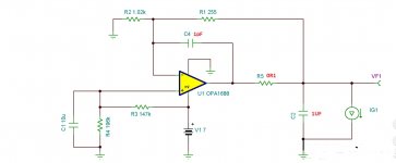
@sciencesky, We haven't been talking about headphone amps (I don't think). Believe that the opamp schematic a few posts up using OPA1688 is for a reference voltage supply, or something of that nature.
Interesting, Mark - have you got a link to further reading on this, please?
Nope, sorry. It was via 'private communication,' as they say.
Nope, sorry. It was via 'private communication,' as they say.
OK, understood - sorry, I thought the bit about seeing ringing on the PS was an investigation posted publicly.
I notice mention was made of the ES9018k2m DAC chip earlier in the thread as used in the Topping D10 (which doesn't suffer from the ESS hump). Is discussion of this just going to dilute this thread as I have done a brief analysis of the board & can post my thoughts on its weakness & possible areas for improvements - if there's any interest?
...I have done a brief analysis of the board & can post my thoughts on its weakness & possible areas for improvements - if there's any interest?
Sure, go for it 🙂
Why not post a new thread about ES9018K2M.I notice mention was made of the ES9018k2m DAC chip earlier in the thread as used in the Topping D10 (which doesn't suffer from the ESS hump). Is discussion of this just going to dilute this thread as I have done a brief analysis of the board & can post my thoughts on its weakness & possible areas for improvements - if there's any interest?
This thread is about ES9068Q2M board.

@zek, All Sabre dacs are basically the same. There are a few differences, but what one needs to know to make one sound good often applies to all of them. Same for AK4499 in certain respects since it is also a switched-resistor current-output dac. Output stages and AVCC or Reference Voltage power supplies have common considerations for all of them.
If one pays attention, it is all of use for making improvements for ES9038Q2M dacs.
If one pays attention, it is all of use for making improvements for ES9038Q2M dacs.
The Topping D10 is a good base for modding based on price & build quality as well as the fact that it measures well. So I bought one to see/hear what this can deliver & see if it can be audibly improved. The sound is pretty much the same as what you get with most DACs these days - all the note sin the right place & nothing obviously wrong with it but it fails to go the extra step which is possible with DACs & provide a more realistic & more engaging sound which holds attention & conveys the emotional aspects in the music.
I've analysed the board but haven't done any modifications to it yet so it may be that ultimately it can't be audibly improved?
Here are the notes I made:
There seems to be two versions of the pcb that I've discovered so far
Here's a pic of the older pcb -mine has another linear regulator (1V) between the two 3.3V Vregs seen in the pic below the ESS chip

All regulators use Vbus power as input - no pre-regulation - nice ground island for each area - XMos, ESS, display, output stage
XMOS chip
ES9018k2m DAC chip
Other notes
Possible areas for improvement/Experiments/discussion:
edit:
Sorry zek, I missed your post while I was putting this together
As Mark says though, what applies to one ESS chip. board often applies (or can be used) on other ESS based boards - for instance
But if the consensus is a separate thread then so be it
I've analysed the board but haven't done any modifications to it yet so it may be that ultimately it can't be audibly improved?
Here are the notes I made:
There seems to be two versions of the pcb that I've discovered so far
Here's a pic of the older pcb -mine has another linear regulator (1V) between the two 3.3V Vregs seen in the pic below the ESS chip
All regulators use Vbus power as input - no pre-regulation - nice ground island for each area - XMos, ESS, display, output stage
XMOS chip
- TPS54231 Dc-Dc converter (8 leg chip) generates 1V directly
- 1V is power on a number of XMOS pins
- No separate 1V for PLL_AVDD as recommended by XMOS - no RC filter either on this pin so a definite weakness
- 3.3V (labelled USB 3.3V) is generated with linear Vreg & used in XMOS
- 24MHz clock used - powered by USB 3.3V?
ES9018k2m DAC chip
- Liner Vregs for 1.2V & 3.3V
- 100MHz clock is used so internal ASRC is being used i.e. asynch mode
Other notes
- Two audio clocks 22.xxxx & 24.xxx are on board (powered by "USB 3.3V") - these are both permanently enabled & powered - the output clock signal runs through two flipflops which switches the clock signal to MCLK - the enable signal probably comes from XMOS chip - I haven't traced this
- Output stage uses TPS65130 dc-dc reg to generate +8V & -8V for opamps
- Power for display is generated through a linear Vreg 3.3V
Possible areas for improvement/Experiments/discussion:
- Provide clean 5V power instead of VBUS - easy to do
- Provide 1V power to PLL_AVDD using linear vreg - can be provided at 1V test point (need to turn off power to the dc-dc converter)
- See if audio clock signals can be routed to ESS MCLK input instead of 100MHz clock - turning it into synchronous operation - I believe this automatically bypasses the internal ASRC without any register changes. Synch clocking on ESS chips is audibly better once a low jitter I2S signal is at the input
- Replace 1V DC-DC reg with linear Vreg
- Separate 1V power to PLL_AVDD pin 39 of XMOS chip - connection point can be easily? exposed by removing 0R chip
- Down the road - output stage - replace dc-dc converter giving +/-8V to opamps or replace output stage completely?
- I haven't looked at ESS AVcc supplies yet but they are supplied by linear regs - BTW ESS9018k2m datasheet can be found on-line 🙂
edit:
Sorry zek, I missed your post while I was putting this together
As Mark says though, what applies to one ESS chip. board often applies (or can be used) on other ESS based boards - for instance
But if the consensus is a separate thread then so be it
Last edited:
merrill, do you have a datasheet for that particular ESS chip? I don't.
I do see lots of problems and not enough ground plane real estate to fix them all.
Looks like another one of those dacs like Khadas tone board that is designed to measure well first, and do so at a low price point. That means sound quality is not a consideration for anything, only the numbers that will be measured matter. What you get is what the numbers alone sound like.
If you want a good ESS dac for cheap (<$200), I think Allo's new USB dac might be the one to watch out for. We'll have to see though. Don't have one here to review yet. Expected to measure extraordinarily well and sound good too, that's the goal anyway as it has been described to me.
Last edited:
Mark,
Easy to find on first page of google search results for "Es9018k2m datasheet"
Under the board the ground plane islands are nicely arranged - keeping each function separate & in it's own domain
I agree that it is designed to measure well, aren't most DACs that follow datasheet recommendations?
But it is well done, nice pcb, lots of test points where signals or power can be injected.
You may be correct that there is no improving it but I thought I would post my thoughts anyway & if I do find improvements, I will report back. I noted that the previous modification which was mentioned on this thread & which it was stated greatly improved the sound, was the 1V power to the XMOS chip. After looking into the design this doesn't surprise me as it is generated on-board by the 1V dc-dc converter - an obvious weakness
One thing to note about my suggestion of going synchronous with the clock into the ESS chip is that DSD needs greater than 27MHz when 1.8V is at DVCC pin & >50MHz if 3.3V is used.
Last edited:
DSD needs greater than 27MHz when 1.8V is at DVCC pin & >50MHz if 3.3V is used.
We seem to be interpreting that part differently. There is no requirement for particular frequencies, rather there is a requirement for particular power supply combinations at higher frequencies. That's still the case to some extent with newer chips in the same line and for other high speed devices. Basically, some parasitic/intrinsic capacitances inside the chip are fixed. Running at higher frequencies requires that the capacitances be charged up more rapidly, and that takes a bit more voltage. That's the nature of the info I think you have probably been looking at.
Last edited:
Yes sorry about that - my mistake - I read it completely wrong - DSD support is fine once MCLK > 3*FS so we are golden
What I should have said - If DVCC is 1.8V & MCLK <27MHz then 1.2V DVDD is supplied internally. If MCLK >27MHz then 1.2V DVDD has to be supplied externally
Same applies when DVCC is 3.3V but limit is now 50MHz
I don't know how that board in the pic worked as it has no 1.2V regulator that I can see (unlike my board) & the clock is 100MHz - same as clock on my board - so external DVDD would be needed??
Any idea what I'm missing - could be on underneath of board, I guess?
What are the other problems you see - ESS AVCC supply?
This is the board I have with 1.2V regulator
Last edited:
Any idea what I'm missing?
What are the other problems you see - ESS AVCC supply?
Perhaps first board was built from very preliminary data.
--------------------------------------------------
Basic dac board upgrade considerations:
Conversion to external linear power supplies. (No wall warts or DC-DC converters allowed)
Dedicated, individual voltage regs of good quality for everything that should have it: DVCC, VCCA, AVCC, Clock, etc. as applicable for specific chip.
Stereo AVCC supplies along the lines of what ESS recommends (but with low noise reference 3.3v added before buffer opamp input filter): http://www.esstech.com/files/4514/4095/4306/Application_Note_Component_Selection_and_PCB_Layout.pdf
Ground plane usage and layout as per above document.
Standard 3-opamp output stage per same document as above, but using OPA1612, and possible substitution of MFB differential summing stage topology (probably lower distortion, better sound quality possible).
Clock upgrade and dedicated clock voltage regulator (possible conversion to synchronous/master operation if register programming is included in project).
Register programming for best sound quality. Arduino works fine.
Last edited:
- Home
- Source & Line
- Digital Line Level
- ES9038Q2M Board