Try here:
??????????????
The Japanese gentleman has done some work with 9038 (and lots of other stuff). Google translate is your best friend.
Then there's Mercury I/V stage from Twisted Pear guys.
If I were to do it, I would take a nice FET input opamp (OPA1656 or better yet OPA828) and pair it with LME49600 (like for headphone amplifier) and use it as I/V converter. Filter values you can find in 9038 8 channel EV board.
Good luck
Hello,
Have tried to find a schematic for a stereo output stage for the pro version of 9038.
The official ESS evaluation board drawing package is freely available for download. It includes a schematic, BOM, gerbers, and the whole PCB design package (which is based on Diptrace PCB design software).
DipTrace - Schematic and PCB Design Software
https://ismosys.com/wp-content/uploads/2020/08/ES9038PRO-8CH-Ver-1.3.zip
Mostly, what's different is that ES9038 PRO runs at high AVCC current, so the AVCC power supply, the output stage opamps, etc., have to be chosen with that in mind. The only difference between ES9038 PRO and ES9028 PRO is AVCC currrent output stage opamp current. IMHO its easier to design a good AVCC supply for 9028PRO. The downside would be a little higher noise level due to the higher output impedance.
Last edited:
Please see attached. However, I wouldn't do it exactly like they did, and pretty sure at least some other people around here have their own approaches that are probably better the ESS design. The evaluation board design is to show off the bells and whistles, and how little it takes to make a dac with their parts. You know. Maybe for asynchronous USB you might want to turn off the ASRC and go with synchronous mode instead.
Attachments
yes, compactness and only single-endedOptimal in what way? Compactness? Do you need both balanced and single-ended?
Well, the ESS schematic can be used, but without the XLR output opamps. Other things that you might want to consider include some of the voltage regulators, which can have a significant effect on sound. And or whether or not to use two clocks, and where those clocks would be located. Is this going to be used with USB intput, or SPDIF, or what? Are you going to include an MCU to adjust the dac chip control registers (which is highly recommended)?
Okay. That raises some questions, seems like. Does SQ matter at all, or only compactness? If SQ isn't to be sacrificed more than necessary, then there is a question about how everything gets clocked and the number of sample rate conversions that the audio stream will be processed through. Say, if you set you SBC to output audio at 96kHz, then you use a USB to I2S board to connect the computer ADAU I2S inputs. Then if ADAU is to run at 96kHz with its own clock, and then if ES9038PRO runs with its own clock, then the audio is going to have clearly more noise and distortion that it originally did.
Say, for example, assuming you need to run the ADAU at a fixed sample rate then it would be much better to limit the system to one synchronous sample rate conversion, and only one clock domain. Not sure if you are already familiar with all that, but kind of seems like maybe you aren't since you mentioned a 100MHz clock as one option. Already that implies more than the minimum number of clock domains. Before I go on, do you care about any of this and or do you want me to go on?
Say, for example, assuming you need to run the ADAU at a fixed sample rate then it would be much better to limit the system to one synchronous sample rate conversion, and only one clock domain. Not sure if you are already familiar with all that, but kind of seems like maybe you aren't since you mentioned a 100MHz clock as one option. Already that implies more than the minimum number of clock domains. Before I go on, do you care about any of this and or do you want me to go on?
Yes, output stage without XLR opamps
voltage regulators - have a solution, will be testet on first prototype PCB
Also use two clocks for test, 100m and 24.576m
i2s input from DSP ADAU, MCU - linux based singleboard computer.
voltage regulators - have a solution, will be testet on first prototype PCB
Also use two clocks for test, 100m and 24.576m
i2s input from DSP ADAU, MCU - linux based singleboard computer.
Attachments
ADAU will be used with fixed samplerate (for example 96khz)Okay. That raises some questions, seems like. Does SQ matter at all, not only compactness.
Say, for example, assuming you need to run the ADAU at a fixed sample rate then it would be much better to limit the system to one synchronous sample rate conversion, and only one clock domain. Not sure if you are already familiar with all that, but kind of seems like maybe you aren't since you mentioned a 100MHz clock as one option. Already that implies more than the minimum number of clock domains. Before I go on, do you care about any of this and or do you want me to go on?
100m clock is saved on test board just for testing, it is assumed that the main generator will be at 24.576 and placed be close to DAC chip,
and both devices adau and the dac.
Yes, you can state your thoughts further.
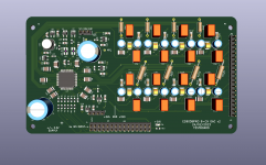
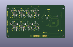
this was to be expected, that's why I posted themThe pictures also raise some questions.
Okay, let's just check a few things if that's okay...
Is there a USB board?
Will the SBC be doing any SRC on the audio stream?
How many layers is the dac board pcb?
Are you familiar with the old ESS app note on board and output stage design considerations?
Maybe I should link to the Gerbers for the ESS evaluation board so you can see what they did there (too much to post so would have to use dropbox or something)?
Are you planning on using a clock buffer chip?
Last edited:
USB not used, SRC via ADAU DSP, PCB 2USB not used, SRC via ADAU DSP, PCB 2 Layers now, Layers now,
About old ESS app note on board and output stage design considerations - I do not remember, may be i've seen it one time, may be not.
Yeah, if it possible i wanna look Eval Board Gerbers (Drobox or Google Drive)
I dont think about clock buffer chip, can you explain it in more details,
Thank you!
About old ESS app note on board and output stage design considerations - I do not remember, may be i've seen it one time, may be not.
Yeah, if it possible i wanna look Eval Board Gerbers (Drobox or Google Drive)
I dont think about clock buffer chip, can you explain it in more details,
Thank you!
- Home
- Source & Line
- Digital Line Level
- ES9038pro stereo outputstage