Hi Everyone!
My newest ESS DAC design is almost finished. I will make a group ordering action if there are any intrested guys in this forum...
Detailed informations are soon available, or please simply ask...!
My newest ESS DAC design is almost finished. I will make a group ordering action if there are any intrested guys in this forum...
Detailed informations are soon available, or please simply ask...!
Attachments

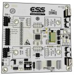
As mentioned, I give a short description of the design. The main goal is to create an affordable, simple but flexibel and very good multichannel DAC system, especially for stereo active speaker systems (like the open baffle LX521 ect...). Earlier I was not a big fan of ESS DACs because of more reasons. The new Hyperstream IV serie brings some benefits indeed, so why not give a try? Some key points:
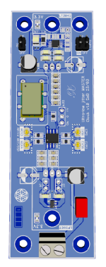
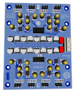
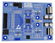
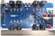
My design as you see contains three main PCBs:
What else is needed to become an operational device:
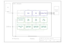
If you wish I can draw a system block schematics for a better visual understanding.
Cheers!
Bela
- The ES9017 and 9027 are both available in "leg" version (QFP package, DIY friendly!) and are pin compatible with each other (THD+N/DNR: 110/120dB vs 114/124dB)
- They can work in hardware mode, so if you don't need any extra options (volume control, ect.) you can use it simply with setting up some jumpers
My design as you see contains three main PCBs:
- the DAC board with all the input/output pins and jumpers, onboard digital regulators
- the Filter board placed directly beneath the DAC, for current/voltage conversation and filtering, as recommended in the datasheet (very special topology!)
- the Clock board with ultra-low jotter oscillator and clock puffer, integrated voltage regulators. It is possible to disable both regulators or even the oscillator and connect external ones.
What else is needed to become an operational device:
- a multichannel digital receiver with I2S outputs (e.g. DIYinhk)
- mains transformers and voltage pre-regulators, especially +/- supply for the opas (I have in my sortiment!)
- 2 pcs of low-noise analog voltage reference regulators (e.g. LT3042, I have in my sortiment!)
- Optional: Micro-controller with IR-receiver and display (e.g. Arduino Nano, I have in my sortiment!)
- Chassis, wires, connectors, ect.
If you wish I can draw a system block schematics for a better visual understanding.
Cheers!
Bela
Because I must drawing it, of course it is not a secret, takes only time... Just as well the costs.Why not a system schema? 🙂
//
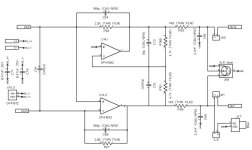
Anyway, the filter topology is just the same like in the manufacturer datasheet. The only difference that I use tht pattern for filter capacitors, to make possible the use of polystyrene caps.
Attachments
First, I am not in the single board community, second, it is not horror, it is very practical for DIY-ers!!! Have you ever developed and mounted a DAC? Have you ever considered the real needs and possibilities?
Yes I have. Many. Since the nineties of last century even. For real needs and possibilities of course. Excessive/unnecessary wiring, crimping connectors and needing to drill and mount several PCBs separated per function for no real reason are all not a blessing. Certainly not for the average DIYer.
But if that is called practical all is good.
But if that is called practical all is good.
Last edited:
Ok, it‘s your opinion. If you make an all-in pcb, you can sink your manufacturing costs, make it smaller and signal integrity will be some better if well designed. Optimal for big companies who have a lot of money and man-time to develope the final circuit and have automated production lines.
BUT for DIY-ers a nightmare!! If you make a design or mounting error somewhere, you can throw away the whole project. You have zero flexibility, if you want to experiment with different components, as filter, oscillator, vregs ect. It is impossible to make a custom tailored setup for your own needs.
The wiring of power supply lines is not an issue, fast, cheap and well-tried. The use of coaxial cables and u.fl connectors for the digital siglans costs somewhat, but I take this, considered the benefits. The analog signal wires or headers can be soldered directly to the pcb if required.
So, it is my way to go certainly! Constructive comments are welcome!
Last edited:
It is possible to design it like the evaluation board (copy-paste), see attached. I must say, it has some aspekts that are not suitable for me, and not to forget the disadvantages I mentioned before. I'll have a solution, where I can drag and drop my DAC+filter (and other components) pcb, and I can change it back with ease to the AK4458, for example. Good luck for soldering this pcb...😉
Attachments
The main benefit is way shorter connections (as in: a fraction). Less board space. Less wiring. Smaller size. It also requires prototyping and skills/experience in improving while doing. An evaluation board by the manufacturer serves another purpose: to evaluate all possibilities and performance. Often used as starting point for a design.
It was not meant to be too negative as most design like this and software also dictates this software way of working. Some think different, I would hate myself for having 3 separate PSU boards and 3 separate transformers but no receiver.
It was not meant to be too negative as most design like this and software also dictates this software way of working. Some think different, I would hate myself for having 3 separate PSU boards and 3 separate transformers but no receiver.
Last edited:
It's ok, I am with you. But this I don't understand why:
"I would hate myself for having 3 separate PSU boards and 3 separate transformers but no receiver."
Of course you can have only one dual output transformer and one PSU board. My phylosophy is to separate the digital and analog sites completely and avoiding all ground loops bw. pcbs. That is my(!) assumption, but technically it can be argumented differently.
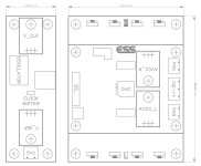
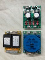
My only consideration was to place the clock near to the DAC chip, see attached my first version. The main reason why I omitted it to an external board was that I couldn't get a proper answer from ESS that the new series ICs have a buffered clock output via GPIO port or not. My requirement is that I will support the DAC and the receiver chip with the same buffered clock signal. Another thought was, if I change the DAC panel, I can keep the clock anyway.
"I would hate myself for having 3 separate PSU boards and 3 separate transformers but no receiver."
Of course you can have only one dual output transformer and one PSU board. My phylosophy is to separate the digital and analog sites completely and avoiding all ground loops bw. pcbs. That is my(!) assumption, but technically it can be argumented differently.
My only consideration was to place the clock near to the DAC chip, see attached my first version. The main reason why I omitted it to an external board was that I couldn't get a proper answer from ESS that the new series ICs have a buffered clock output via GPIO port or not. My requirement is that I will support the DAC and the receiver chip with the same buffered clock signal. Another thought was, if I change the DAC panel, I can keep the clock anyway.
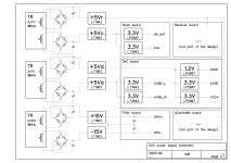
Attachments
- Home
- Group Buys
- ES9017/9027 DAC PCBs