Greetings.
For some time now the need for SMPS powered from the mains power line has become more and more important so i have decided to give it the proper attention, and i have been documented from many sources, and chosen Marty Brown's Power supply cookbook as a guide, but the one thing that got me confused is the error amplifier compensation design, and as regulated voltage at the outputs is verry important, the need to understand this topik becomes verry real, i have read the appendix dealing with this but got left with some confusing subjects and i will state them here one by one and i beg you all to bare with me on this since it is verry important to me.
So let's get down to bussiness, for refference i will name a half bridge forward PSU, with Vin 150V ( on the power transformer primary winding ) and Vout 60V ( the exit to the load voltage ), the power transformer primary winding is of 40 turns and the secondary one is of 32 turns, and i choose an 2 pole 2 zero compensation design, and the first step would be the overall gain of the PSU at DC and a 3 part equation is presented:
My first confusion is right there, to me it seams that every part of the equation gives a different result but still it shouldn't have, first Adc=Vout/Vin in my example it would be 60/150=0,4; second Adc=(Nsec/Npri)*DC and the result i have obtained is (32/40)*(60/150)=0,32; and last Adc=(Vin/Ve)*(Nsec/Npri), and so with a 3V error amplifier range, it would be (150/3)*(32/40)=50*0,8=40;
This is the first step to take in designing the compensation network so it has to be wright, and so i ask of you to clear my confusion, and let me know why are there different results and wich is the actual gain at DC in my example and the correct way to calculate it.
I may seeam simple to you but it has gave me lots of trouble so i need to clarify it, so thank you all for any cind of response.
Regards
Marian.
For some time now the need for SMPS powered from the mains power line has become more and more important so i have decided to give it the proper attention, and i have been documented from many sources, and chosen Marty Brown's Power supply cookbook as a guide, but the one thing that got me confused is the error amplifier compensation design, and as regulated voltage at the outputs is verry important, the need to understand this topik becomes verry real, i have read the appendix dealing with this but got left with some confusing subjects and i will state them here one by one and i beg you all to bare with me on this since it is verry important to me.
So let's get down to bussiness, for refference i will name a half bridge forward PSU, with Vin 150V ( on the power transformer primary winding ) and Vout 60V ( the exit to the load voltage ), the power transformer primary winding is of 40 turns and the secondary one is of 32 turns, and i choose an 2 pole 2 zero compensation design, and the first step would be the overall gain of the PSU at DC and a 3 part equation is presented:
An externally hosted image should be here but it was not working when we last tested it.
My first confusion is right there, to me it seams that every part of the equation gives a different result but still it shouldn't have, first Adc=Vout/Vin in my example it would be 60/150=0,4; second Adc=(Nsec/Npri)*DC and the result i have obtained is (32/40)*(60/150)=0,32; and last Adc=(Vin/Ve)*(Nsec/Npri), and so with a 3V error amplifier range, it would be (150/3)*(32/40)=50*0,8=40;
This is the first step to take in designing the compensation network so it has to be wright, and so i ask of you to clear my confusion, and let me know why are there different results and wich is the actual gain at DC in my example and the correct way to calculate it.
I may seeam simple to you but it has gave me lots of trouble so i need to clarify it, so thank you all for any cind of response.
Regards
Marian.
Seeing as nowone is interested in any cind of answear i helped myself, and reading more thoroughly i found that only the last part of the equation matters in deciding the DC gain, so i started out with the upper example and tested it both graphically and in a simulator ( multisim ), i took in calculation the lowest anticipated Vin witch woulkd be about 86V, the PSU will have a symmetrical output +/-30Vcc, i am monitoring only the possitive rail, and the specs would be:
-Vin(min)=86V
-Vout=30V ( possitive rail monitored )
-Ve=3,5V ( the voltage range of the error amplifier )
-Npri=40 turns
-Nsec=16 turns
The Adc would be:
So Adc=9,82 and Gdc=19,8db.
Now it's time to draw up the LC characteristic, and i have a inductor of 300uH and 2 paralelled filter caps of 1000u each, and a combined ESR of 33m Ohm, so the LC resonance freq would be 205Hz, and the ESR puts a zero at about 2,4Khz, this is the first graphic:
Now, next comes the poles and zeroes, and knowing the PSU's freq is 27Khz i have chosen a crossover freq of 5Khz, and the 2 zeroes at both sides of the Flc, first zero at 40Hz and the second one at 240Hz, the first pole must compensate for the filter caps ESR so it will be at 2,4Khz and the second one needed for stability at high freq, i have chosen it to be at 10Khz, this would be the new graphic with the error amplifier correction drawn in green:
Next step, drawing the global characteristic acoordingly ( the blue line ):
Now the circuit it's self comes to line up, first the schematic :
Second the calculation of the components and testing them in the simulator, and for the sake of the correctness of the simulation i'll imput in multisim the exact values obtained by calculation and if all goes well then i'll choose standard values, so let's get on to it:
-The gaind at the first plateau is of 10db, so the Adc=3,16, and i have alreadu chosen R2 at 2k2, so first the obtained Adc must be assured and at the middle of the plateau it is given by R1/R2 so R1=6,95K ( as i sayd i will stick with theese strange vallues for the time beiyng ).
-The first zero at 40Hz is given by R1+C1, so C1=572n.
-The second zero is at 240Hz with R2+C3, so C3=300n.
-The first pole is at 2,4Khz with R3+C3, so R3=220.
-The second pole is at 10Khz with R1+C2, so C2=2,3n.
Now i have all i need to test it in multisim, and this is what i got:
Error amplifier correction-Amplitude
Error amplifier correction-Phase
The global obtained-Amplitude
The Global obtained-Phase
And this would be all it seams, and to me it seams to be a good method, granted the poles and zeroes can be choosen differently to give the preffered result, and standard values are needed for the components but the fact is this seams to be a good way to calculate it.
What do you think?
Regards,
Marian.
-Vin(min)=86V
-Vout=30V ( possitive rail monitored )
-Ve=3,5V ( the voltage range of the error amplifier )
-Npri=40 turns
-Nsec=16 turns
The Adc would be:
An externally hosted image should be here but it was not working when we last tested it.
So Adc=9,82 and Gdc=19,8db.
Now it's time to draw up the LC characteristic, and i have a inductor of 300uH and 2 paralelled filter caps of 1000u each, and a combined ESR of 33m Ohm, so the LC resonance freq would be 205Hz, and the ESR puts a zero at about 2,4Khz, this is the first graphic:
An externally hosted image should be here but it was not working when we last tested it.
Now, next comes the poles and zeroes, and knowing the PSU's freq is 27Khz i have chosen a crossover freq of 5Khz, and the 2 zeroes at both sides of the Flc, first zero at 40Hz and the second one at 240Hz, the first pole must compensate for the filter caps ESR so it will be at 2,4Khz and the second one needed for stability at high freq, i have chosen it to be at 10Khz, this would be the new graphic with the error amplifier correction drawn in green:
An externally hosted image should be here but it was not working when we last tested it.
Next step, drawing the global characteristic acoordingly ( the blue line ):
An externally hosted image should be here but it was not working when we last tested it.
Now the circuit it's self comes to line up, first the schematic :
An externally hosted image should be here but it was not working when we last tested it.
Second the calculation of the components and testing them in the simulator, and for the sake of the correctness of the simulation i'll imput in multisim the exact values obtained by calculation and if all goes well then i'll choose standard values, so let's get on to it:
-The gaind at the first plateau is of 10db, so the Adc=3,16, and i have alreadu chosen R2 at 2k2, so first the obtained Adc must be assured and at the middle of the plateau it is given by R1/R2 so R1=6,95K ( as i sayd i will stick with theese strange vallues for the time beiyng ).
-The first zero at 40Hz is given by R1+C1, so C1=572n.
-The second zero is at 240Hz with R2+C3, so C3=300n.
-The first pole is at 2,4Khz with R3+C3, so R3=220.
-The second pole is at 10Khz with R1+C2, so C2=2,3n.
Now i have all i need to test it in multisim, and this is what i got:
Error amplifier correction-Amplitude
An externally hosted image should be here but it was not working when we last tested it.
Error amplifier correction-Phase
An externally hosted image should be here but it was not working when we last tested it.
The global obtained-Amplitude
An externally hosted image should be here but it was not working when we last tested it.
The Global obtained-Phase
An externally hosted image should be here but it was not working when we last tested it.
And this would be all it seams, and to me it seams to be a good method, granted the poles and zeroes can be choosen differently to give the preffered result, and standard values are needed for the components but the fact is this seams to be a good way to calculate it.
What do you think?
Regards,
Marian.
Am I seeing a phase of ~180 degrees at ~200Hz at the gain peak (last two pictures)? That sounds bad. Does it run stable in transient sim?
So this is a voltage-mode buck or forward converter, something like that?
I believe the compensator pole must be set below the LC double pole, to reduce gain before the 180 degree phase shift. A single zero is incapable of compensating for this phase shift, since the best you can hope for is still 90 degrees, marginal at best, and the frequency depends on load.
If you implement an inner current-mode loop and wrap the voltage loop around that, you can compensate each individually, breaking the passive LC filter and attaining better dynamics.
Tim
Many thanks for the imput, it is greatly appreciated 😉
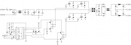
The PSU is a voltage mode, forward half bridge, more precise is a ATX unit modified by me, this is it's schematic (please ignore the values of R11, R32, C3 and C18, these are the ones needed to be calculated ):
I am modifying this unit to power up an BJT audio amplifier with it ( small one as it can bee understud ), about 80W each channel designed by me, but the compensation subject gave me some trouble, and i hope i am at the right track with it.
The phase shift at the gain peak is about +130 deg, i'll attach 2 more pics to ilustrate it:
Gain peak
Phase shift
Now the thing that gets me confused is that abrupt phase shift from about 100Hz to 180Hz, of -170deg, is it normal or the compensation circuit is bad designed?
The PSU is a voltage mode, forward half bridge, more precise is a ATX unit modified by me, this is it's schematic (please ignore the values of R11, R32, C3 and C18, these are the ones needed to be calculated ):
An externally hosted image should be here but it was not working when we last tested it.
I am modifying this unit to power up an BJT audio amplifier with it ( small one as it can bee understud ), about 80W each channel designed by me, but the compensation subject gave me some trouble, and i hope i am at the right track with it.
The phase shift at the gain peak is about +130 deg, i'll attach 2 more pics to ilustrate it:
Gain peak
An externally hosted image should be here but it was not working when we last tested it.
Phase shift
An externally hosted image should be here but it was not working when we last tested it.
Now the thing that gets me confused is that abrupt phase shift from about 100Hz to 180Hz, of -170deg, is it normal or the compensation circuit is bad designed?
An externally hosted image should be here but it was not working when we last tested it.
Last edited:
Ok, so it goes through +/-180 degrees just before the spike. Says gain is 54dB at the peak, which I don't know what that's relative to. If it's the true loop gain, it's certainly oscillating!
Tim
Tim
Your methodology of choosing the error amplifier transfer and calculations of LC poles/zero is well, the professional way.
Good job, it will certainly work fine, the peak at LC resonance is there because of too high a quality of LC-Rload, no worries, there's also no abrupt change in phase, just simulator artifact. In case of any problems try pushing the second zero of error amp (at first amplitude up-slope) a bit lower in frequency.
Good job, it will certainly work fine, the peak at LC resonance is there because of too high a quality of LC-Rload, no worries, there's also no abrupt change in phase, just simulator artifact. In case of any problems try pushing the second zero of error amp (at first amplitude up-slope) a bit lower in frequency.
@darkfenriz thank's allot for the imput and the possitive rating of my work, it means allot and i appreciated.
Now at the crossover freq of my choosing ( 5Khz ) the phase shift is about +60deg, as i understand the goal is to get as close as possible to 45, so i need to ask this, do i need to improove the PS or 60deg is still a working value? and if the phase shift needs improoving then what do you think would be the best way to do it?
Regards,
Marian.
45 deg of phase margin at crossover (0dB magnitude) is just a thumb rule, usually a good compromise between safety of not going unstable and performance.
Less than 45 deg is squeezing faster transient response while risking it goes wild under certain conditions (inductance drop, low line, high line, low load, high load etc.), more than 45 deg is more margin and less performance. The choice is all yours.
Less than 45 deg is squeezing faster transient response while risking it goes wild under certain conditions (inductance drop, low line, high line, low load, high load etc.), more than 45 deg is more margin and less performance. The choice is all yours.
Ok got it, as i have seen in simulation increasing just a bit the vallue of C2 from the schematic in #2 post results in less phase margin, so i think by choosing the standard vallues of the components and some compromise, a good working PSU cand be obtained. Thanks again for the imput.
Now as i sayd in the first post my goal is to design and built from scratch a good-reasonable PSU, that ATX is about done, just needs some finishing touches, so the main reason i have come with this subject here is because i intend to desighn and built a new one, i need at it's outputs +/-50Vcc regulated, and the current limmit will be set at about 10A at witch point the PSU will block and need reset, last night i started the schematic and chosen an Push-Pull topology to avoid the need for driver transformer, the power switches will be mosfet ( i have not decided exactly witch one to use, maybe IRFPC60 ), i haven't had the time to choose the power transformer yet, nor did i calculated stuff like snubbers, compensation and such, they will be calculated at the wright time, for the moment i've just put some bits and pieces together and i will show you all what, and await your imput, i will power the IC and bias circuit from an auxiliary PSU, be it a simple flyback or just a small transformer that remains to be seen later, this way i will not need opto ( and all it entails ) on the feedback network. I know it is sort of a mess there but i will estetize it more along the way.
Now as i sayd in the first post my goal is to design and built from scratch a good-reasonable PSU, that ATX is about done, just needs some finishing touches, so the main reason i have come with this subject here is because i intend to desighn and built a new one, i need at it's outputs +/-50Vcc regulated, and the current limmit will be set at about 10A at witch point the PSU will block and need reset, last night i started the schematic and chosen an Push-Pull topology to avoid the need for driver transformer, the power switches will be mosfet ( i have not decided exactly witch one to use, maybe IRFPC60 ), i haven't had the time to choose the power transformer yet, nor did i calculated stuff like snubbers, compensation and such, they will be calculated at the wright time, for the moment i've just put some bits and pieces together and i will show you all what, and await your imput, i will power the IC and bias circuit from an auxiliary PSU, be it a simple flyback or just a small transformer that remains to be seen later, this way i will not need opto ( and all it entails ) on the feedback network. I know it is sort of a mess there but i will estetize it more along the way.
Attachments
I know that the voltage rating of the mosfets can be a real problem in push pull, but half bridge for 1KW of power it would be a bit of too much i guess😕...maybe full bridge but it is sorf of more complex.
Sorry for the double post but i cannot edit the last one...🙁
So, estimating an efficiency of 80% means that the power switches will have to handle about 1,25KW of power, and as the voltage on the wall socket sometimes goes down to about 190V that means the power mosfets will have to handle about 9-10A, is it not a bit too much? i think maybe at least 3 pairs each of mosfets to be on the safe side, am i wright?
So, estimating an efficiency of 80% means that the power switches will have to handle about 1,25KW of power, and as the voltage on the wall socket sometimes goes down to about 190V that means the power mosfets will have to handle about 9-10A, is it not a bit too much? i think maybe at least 3 pairs each of mosfets to be on the safe side, am i wright?
- Status
- Not open for further replies.
- Home
- Amplifiers
- Power Supplies
- Error amplifier compensation desighn in SMPS